Chain Architecture
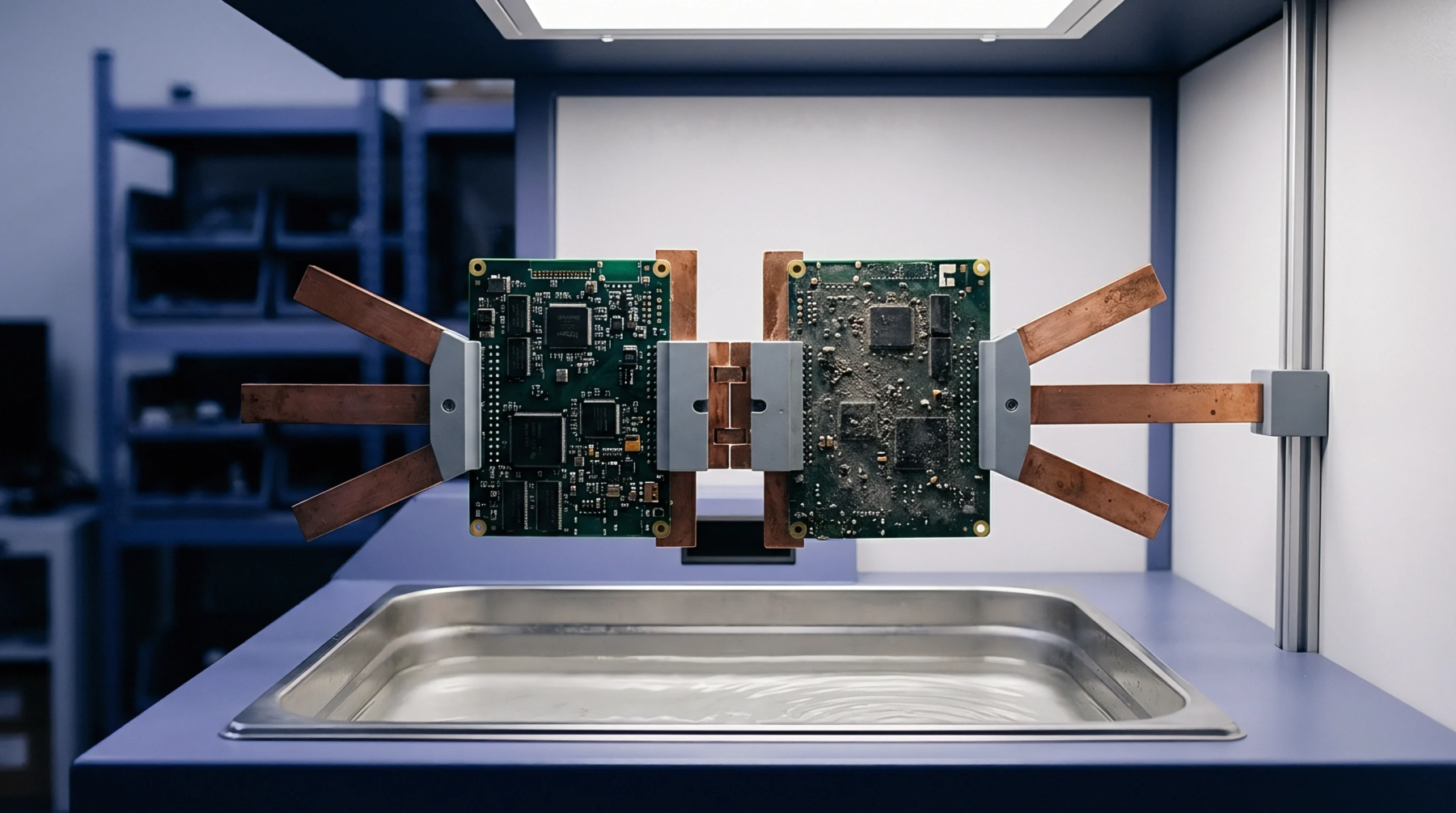
Serial interconnection schemes in electronic design link the boundary scan structures of multiple integrated circuits into a single loop. The implementation of multi-chip chain concatenation establishes a continuous data path where the test data output of one device feeds the test data input of the next.
Signal Flow
Clocked data shifts through every connected device in the chain under the control of a single test access port controller. In a multi-chip chain concatenation setup, the length of the instruction and data registers grows with each added device. This larger register chain requires the test system to calculate the correct instruction lengths to properly target a specific integrated circuit during tests.
System Integrity
Physical layouts of complex printed circuit board assemblies utilize these long serial paths to minimize the number of test access points required on the board. When troubleshooting board-level defects, the test software shifts diagnostic patterns through the concatenated path to pinpoint the exact pin that has failed. If any single device in the chain becomes unpowered or damaged, the entire serial loop breaks, halting all boundary scan activities.
Designers evaluate these chains to ensure that noise and clock skew do not degrade the high-speed test signals. Protecting this path guarantees continuous testability across all assembled board components.