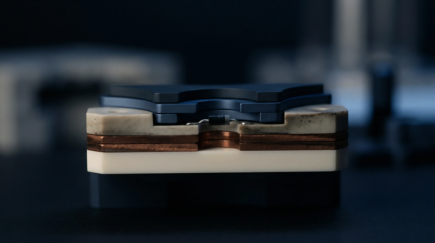
Internal Imaging
Ultrasonic sound waves provide a longitudinal view of internal structures by measuring the time of flight for echoes returning from interfaces of varying acoustic impedance. This b-scan cross section produces a two-dimensional slice through a circuit board or semiconductor package to identify layer registration or internal delamination. Acoustic energy travels from a transducer through a coupling medium to illuminate boundaries between different materials.
The depth of every interface appears on the screen based on the speed of sound through the specific medium. Operators gain insight into the structural integrity of buried features by reviewing the intensity and location of these return signals.
Acoustic Limitation
Precision in this measurement depends upon the frequency of the transducer and the homogeneity of the materials under test. Higher frequencies offer superior resolution for smaller defects but suffer from greater attenuation within thicker or more absorbent substrates. A b-scan cross section requires a clear path for sound propagation, which prevents its use on components with high porosity or massive air voids that scatter energy.
Proper selection of the pulser and receiver settings governs the detection limit of the underlying scanning system.
Assembly Verification
Quality control protocols rely on this non-destructive method to validate the condition of flip-chip bumps and die-attach layers after thermal reflow processes. The resulting image identifies voids in thermal interface material and misalignment of conductive features that escape visual inspection. A b-scan cross section documents the physical state of the connection without requiring mechanical sectioning of the assembly.
Manufacturers apply these scans to confirm that internal junctions remain intact following environmental stress testing.