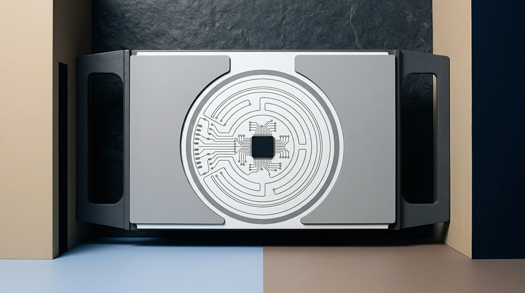
Surface Flattening
Polishing technique removes excess material from a semiconductor wafer to achieve a global topography that is flat within nanometer tolerances. During the manufacturing of multi-layer circuits, chemical mechanical planarization combines abrasive slurry chemistry with mechanical force to grind away high points on the surface. It ensures that the focal depth of lithography tools remains consistent across the entire diameter.
The process stops when the target thickness or a stop layer is reached, which prevents damage to the underlying circuit structures.
Material Removal
Rotary pads and chemically active fluids work together to dissolve and shear away metal or dielectric layers. Pressure and velocity determine the rate at which chemical mechanical planarization eliminates surface irregularities. If the slurry pH is incorrect, the removal rate becomes unpredictable and leads to surface defects.
Planarity Impact
Uniformity across the wafer determines the success of subsequent etching and deposition steps. When chemical mechanical planarization fails to create a level surface, metal lines may short or break due to step coverage issues. Inspection tools verify the post-polishing height to confirm that the substrate meets the flatness requirements for high-density interconnects.
Failure to maintain this planarity causes errors in the electrical performance of the final device.