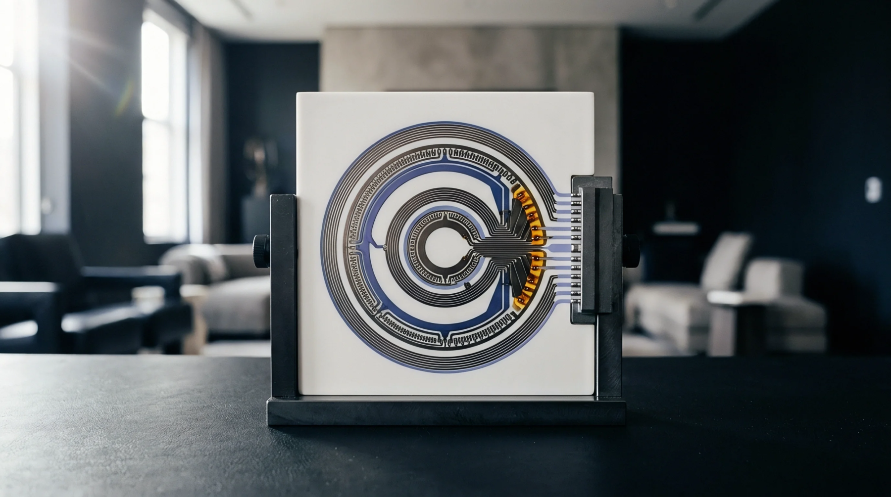
Thermal Insert
Solid metallic inserts integrated directly into printed circuit board substrate cavities provide localized conduction pathways for high-dissipation semiconductor packages. Manufacturing engineers position the embedded copper coin beneath power amplifier or regulator footprints to transfer heat directly through multilayer cores into chassis heat sinks. Pure electrolytic copper provides thermal conductivity exceeding three hundred and eighty watts per meter-kelvin, bypassing resin-rich prepreg limitations.
The coin geometry spans rectangular, T-shaped, or cylindrical forms mechanically routed or pressed into pre-drilled cavity structures. Bonding methods employ sweat-soldering, galvanic plating, or high-conductivity structural adhesives to secure coin margins to internal copper planes. Mechanical tolerance matching between the laminate cutout and the copper insert prevents resin squeeze-out or surface depression during multilayer lamination cycles.
Lamination Integration
Fabricators seat the machined insert into pre-routed inner-layer cores prior to final vacuum press cycles. Integrating an embedded copper coin requires prepreg plies micro-routed with matching clearance pockets to prevent resin starvation around the solid metal perimeter. Differential thermal expansion between dielectric glass-epoxy matrix laminates and the solid copper slug induces internal shear stresses during high-temperature press cure.
Planarity across the finished outer surface dictates whether subsequent surface mount assembly completes reliably. Controlled-depth mechanical brushing and planarization grinding remove protruding copper flash before surface plating deposition. Chemical etching steps clean the interface lines, securing adhesion between the coin edges and surrounding prepreg resin.
Interface Verification
Quality acceptance protocols measure planar topography, interface voiding, and galvanic continuity between the insert and adjacent reference layers. Surface height variation across the embedded copper coin boundary must not exceed twenty-five micrometers to prevent stencil standoff gaps or component rocking during reflow. Cross-section metallography checks joint integrity between plated hole walls and coin perimeters.
Acoustic microscopy or non-destructive x-ray imaging reveals delamination along vertical resin interfaces following repeated thermal shock testing. Excessive air gaps around the coin periphery impede lateral thermal dispersion and cause solder blowholes during downstream assembly reflow.