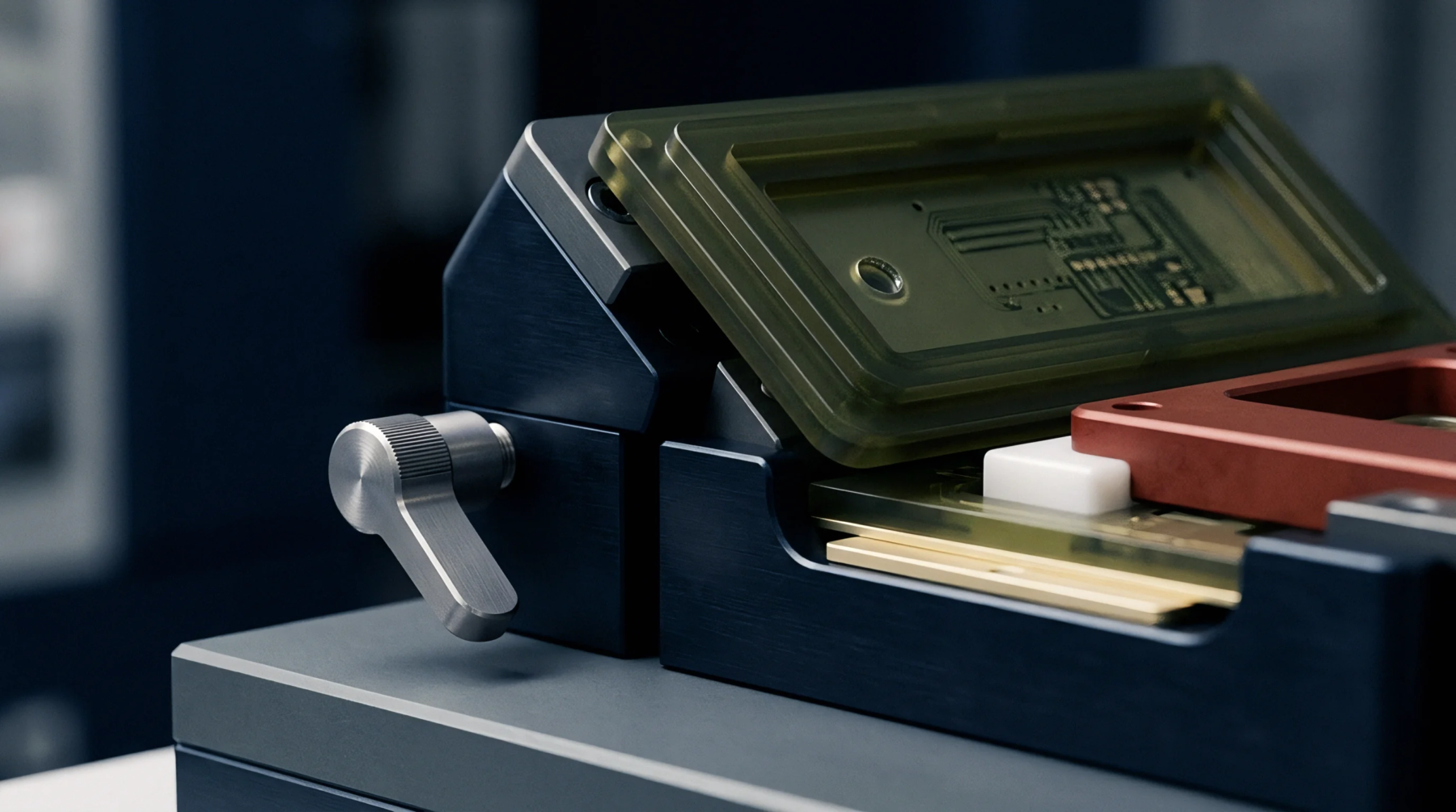
Structural Arrangement
The sequential ordering of copper foils and dielectric cores determines the electrical performance and the physical thickness of a multilayer circuit board. An inner layer stackup specifies exactly where ground planes and signal traces sit within the finished assembly. Fabricators use this blueprint to ensure that the impedance of high speed lines meets the design requirements.
This configuration must account for the thickness of the prepreg layers that bond the various cores together during the final lamination press.
Electrical Influence
Controlling the distance between signal traces and their return planes is the primary method for managing characteristic impedance. Within an inner layer stackup, the dielectric thickness between a trace on layer three and a ground plane on layer two must be kept within tight tolerances. If the spacing varies during the pressing process, the impedance will deviate from the target value, potentially causing signal reflections or data errors in high frequency circuits.
Fabrication Sequence
Balancing the distribution of copper across the layers prevents the board from bowing or twisting after it leaves the press. A lamination plan that places heavy copper on one side and light signal density on the other will likely result in measurable warpage.