Scanning Acoustic Microscopy Characterization of Semiconductor Package Interface Integrity
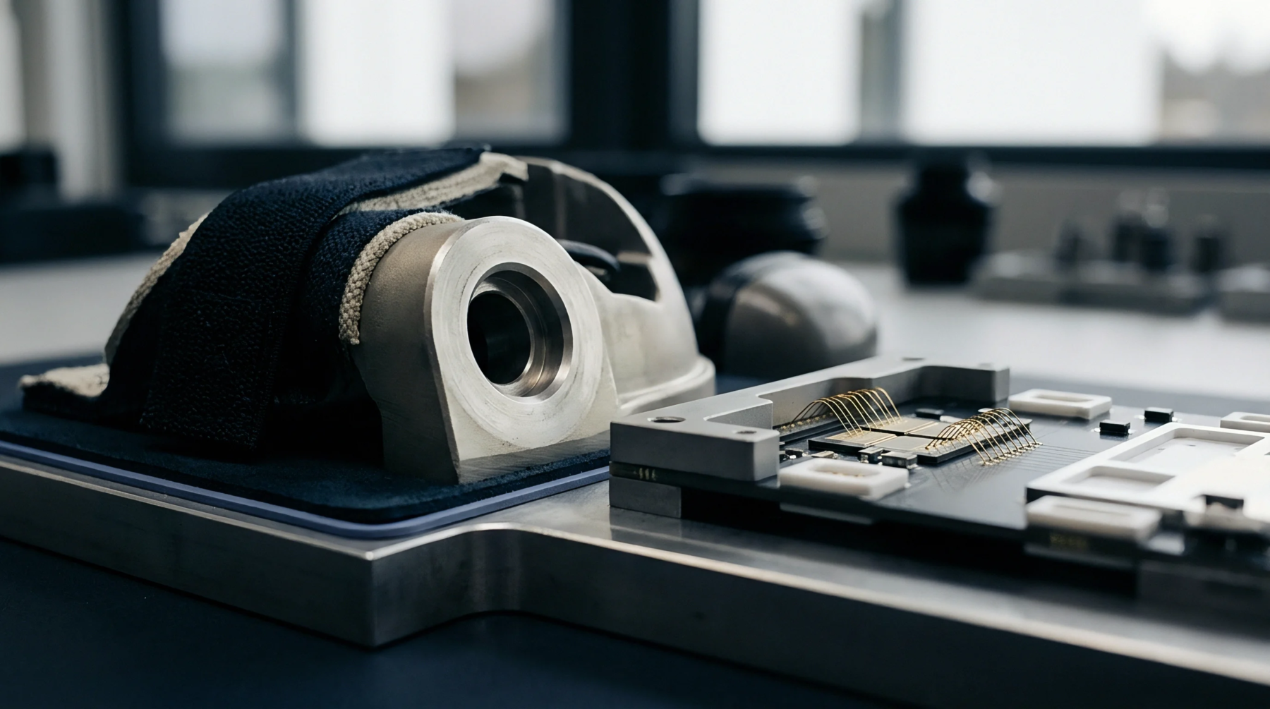
Acoustic microscopy verifies semiconductor package interface integrity by tracking reflection phase inversion and amplitude shifts across gated depth planes.
Acoustic microscopy verifies semiconductor package interface integrity by tracking reflection phase inversion and amplitude shifts across gated depth planes.
Expertise is a utility, not a secret. sentiention™ publishes its working knowledge as open reference: intelligence layer covering the materials it sources, the markets it enters, and the reference that serves both.