Edge Clearance
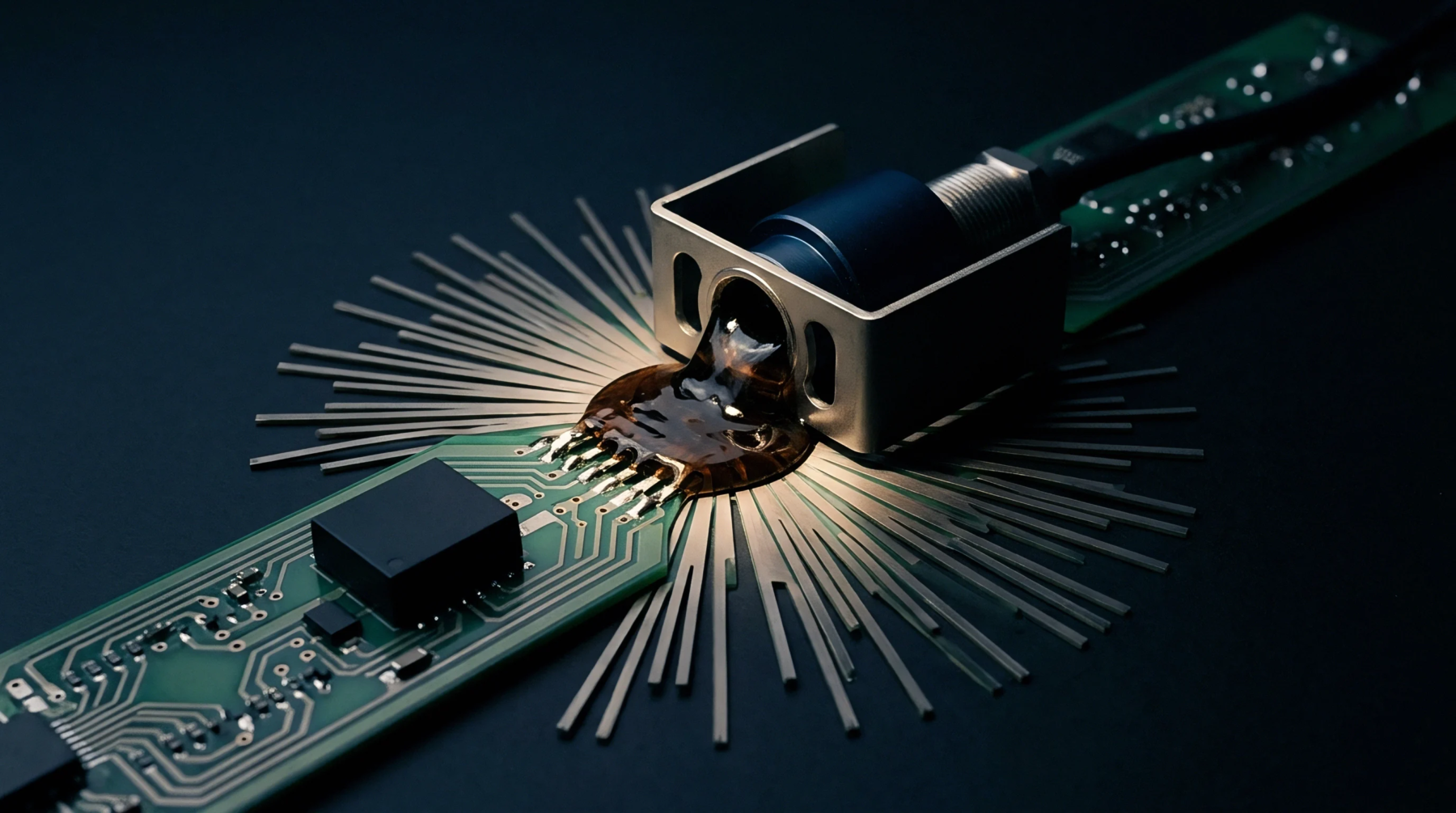
Insulation at the edges of a printed circuit board is maintained by stopping the internal copper layers a short distance from the physical boundary of the panel. Power plane pullback prevents the conductive copper from being exposed during the routing or dicing process, which could lead to short circuits or corrosion. This clearance is also required to satisfy safety standards for creepage and clearance distances between high voltage areas and the chassis.
Safety Requirement
Dielectric breakdown at the board edge is avoided by ensuring the power layers do not extend into the area where the mechanical cutting tool operates. This power plane pullback creates a protective margin of resin that seals the copper from the environment.
Manufacturing Tolerance
Precise control over the routing path ensures that the distance from the copper edge to the board profile remains consistent. When the power plane pullback is too small, the copper might be smeared by the router bit, creating a potential path for an electrical arc. Standard design rules often specify a minimum clearance of zero point five millimeters, though this may increase for high voltage applications.
Fabricators check this dimension during the automated optical inspection of internal layers. If the copper extends too far, the panel may be rejected to prevent reliability issues in the field. This margin also accounts for the slight registration errors that occur when the different layers are stacked and pressed together.