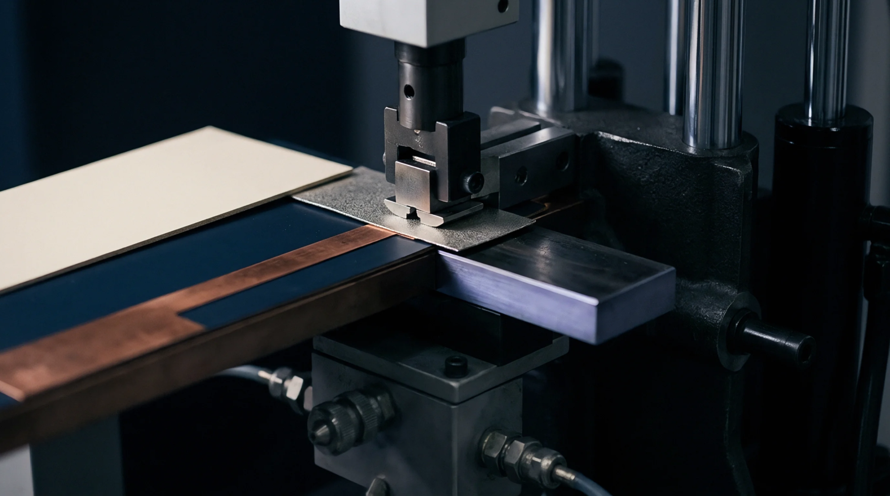
Trace Optimization
Adjustment of trace dimensions and dielectric spacing on high-speed printed circuit boards prevents signal distortion and reflection along transmission lines. Implementing signal impedance control ensures that the trace matches the source and load impedances of the active components. This technique is necessary for high-frequency designs where signal integrity is a major concern.
Designers specify target impedance values, typically fifty or ninety ohms, on their fabrication drawings.
Dimensional Variable
Physical parameters such as trace width, copper thickness, and dielectric height dictate the characteristic impedance of a conductor. When manufacturing boards with signal impedance control, fabricators must maintain tight tolerances on these physical features. Changes in trace width or dielectric thickness can shift the impedance outside the acceptable tolerance.
Verification Method
Testing of dedicated test coupons situated on the panel edge allows fabricators to verify trace performance without damaging the production boards. Time-domain reflectometry measures the impedance of these coupons by sending a fast electrical pulse down the line and analyzing the reflected wave. If the measured impedance deviates from the specified range, the board fails inspection.
Adjusting the etching process during trace formation allows fabricators to correct for slight variations in copper thickness. This real-time feedback ensures that every production panel meets the requirements of high-speed digital networks. Consistent control of trace geometry guarantees uniform performance across all manufactured batches.