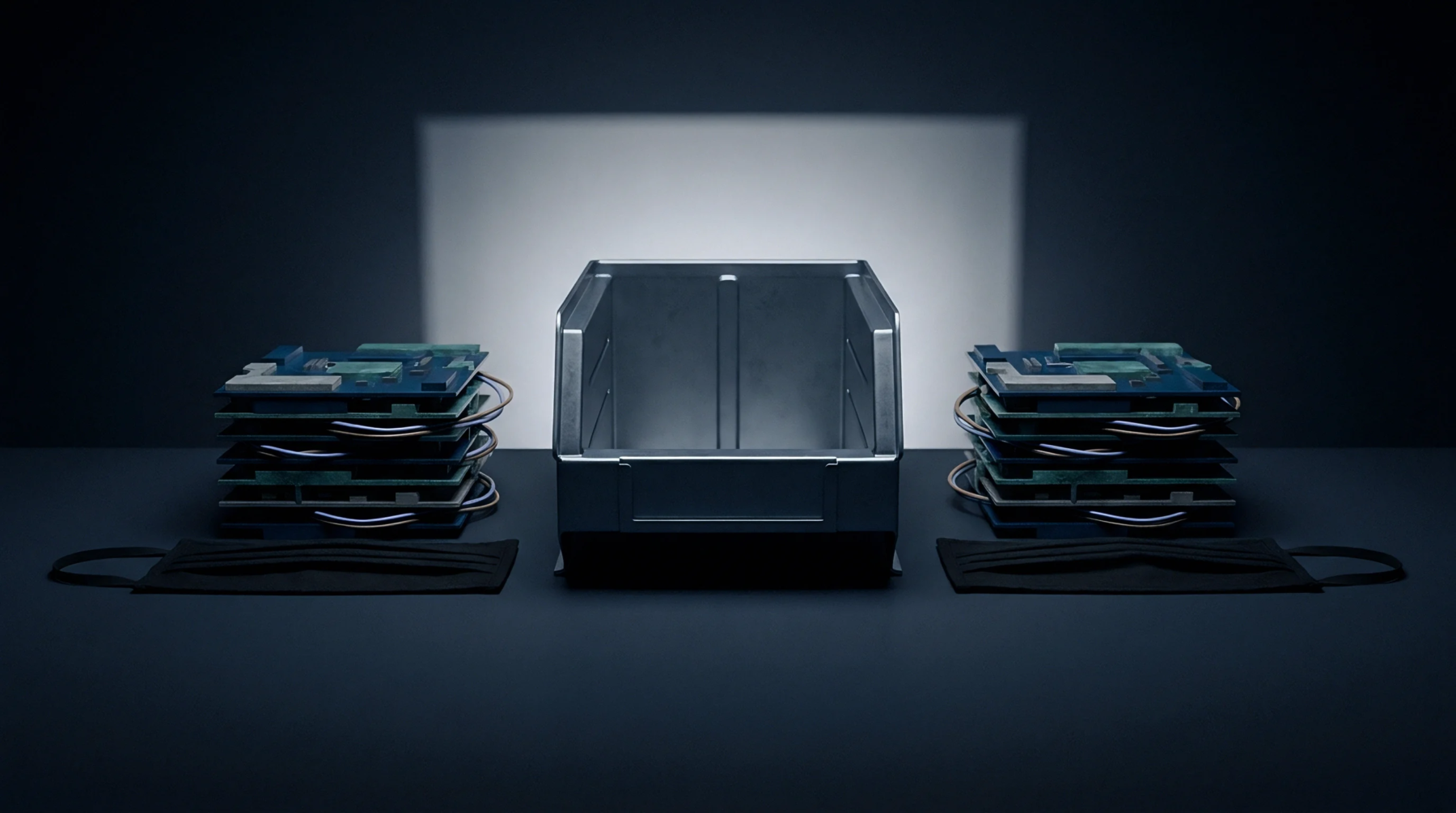
Interconnection Failure
Defects in the surface-mount assembly of printed circuit boards can prevent the necessary electrical connection between components and substrate pads. The occurrence of solder opens designates physical separations where the solder paste failed to wet or bridge the gap between the electronic component terminal and the board pad. This results in an incomplete electrical circuit and subsequent system failure.
Assembly Origin
Several factors during the printing and reflow stages of assembly can lead to these disconnected joints. Incorrect stencil thickness or blocked stencil apertures can deposit insufficient solder paste on the pads, which leads to solder opens when the components are placed. Warpage of the circuit board during the high-temperature reflow cycle can also lift component pins away from the melting alloy before it solidifies.
In addition, oxidization of either the component lead or the board pad will prevent the solder from flowing and bonding correctly.
Inspection Method
Automated optical inspection systems scan the boards after the reflow oven to catch these gap defects before final potting or enclosure assembly. When the defects are hidden beneath area array packages like ball grid arrays, x-ray inspection must be used to view the internal joints. Resolving these failures requires manual touch-up with a soldering iron or running the affected board through a dedicated hot-air rework station.