Measurement Geometry
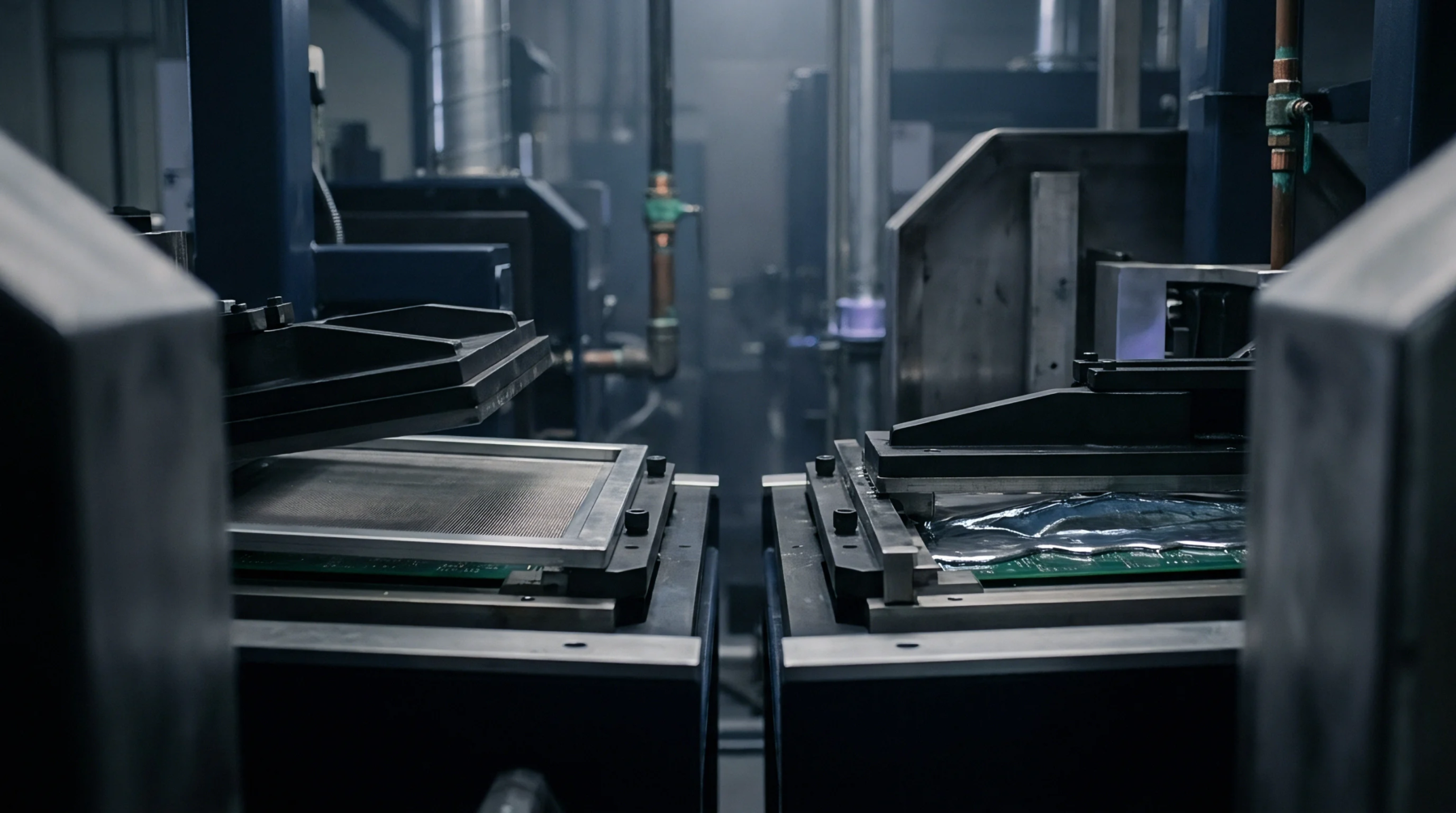
Geometric deviations on a solid interface determine the contact area and frictional behavior between adjacent components in high density assemblies. Surface topography quantifies these irregularities by recording the height distribution of peaks and valleys across a defined spatial region. This characterization identifies deviations from nominal flatness that impede solder paste deposition or chip attachment.
Accurate profile acquisition requires non contact scanning methods like laser triangulation or optical interferometry to prevent mechanical damage to delicate copper features. Instruments generate a digital elevation map by sampling point clouds at micron scale resolution.
Fabrication Requirement
Mechanical stability depends on the depth and orientation of grooves left by chemical milling or abrasive finishing steps. Variations in these microscopic textures influence the wetting angle of molten alloys during reflow cycles. Boards with excessive roughness trap voids at the interface which diminishes thermal conductivity between the die and the substrate.
Process engineers monitor these parameters to confirm that surface finishes adhere to the roughness average specifications required for reliable electrical connectivity.
Interface Verification
Inspectors evaluate the compliance of printed boards against predefined arithmetic mean deviation standards during final quality control. Higher deviation values signal instability in the etch process that promotes peeling or delamination under environmental stress. Data extracted from these profiles correlate directly with the long term structural integrity of the solder joints.
Final readings provide the evidence necessary to approve or reject a batch based on its physical fitness for assembly operations.