Heat Dissipation
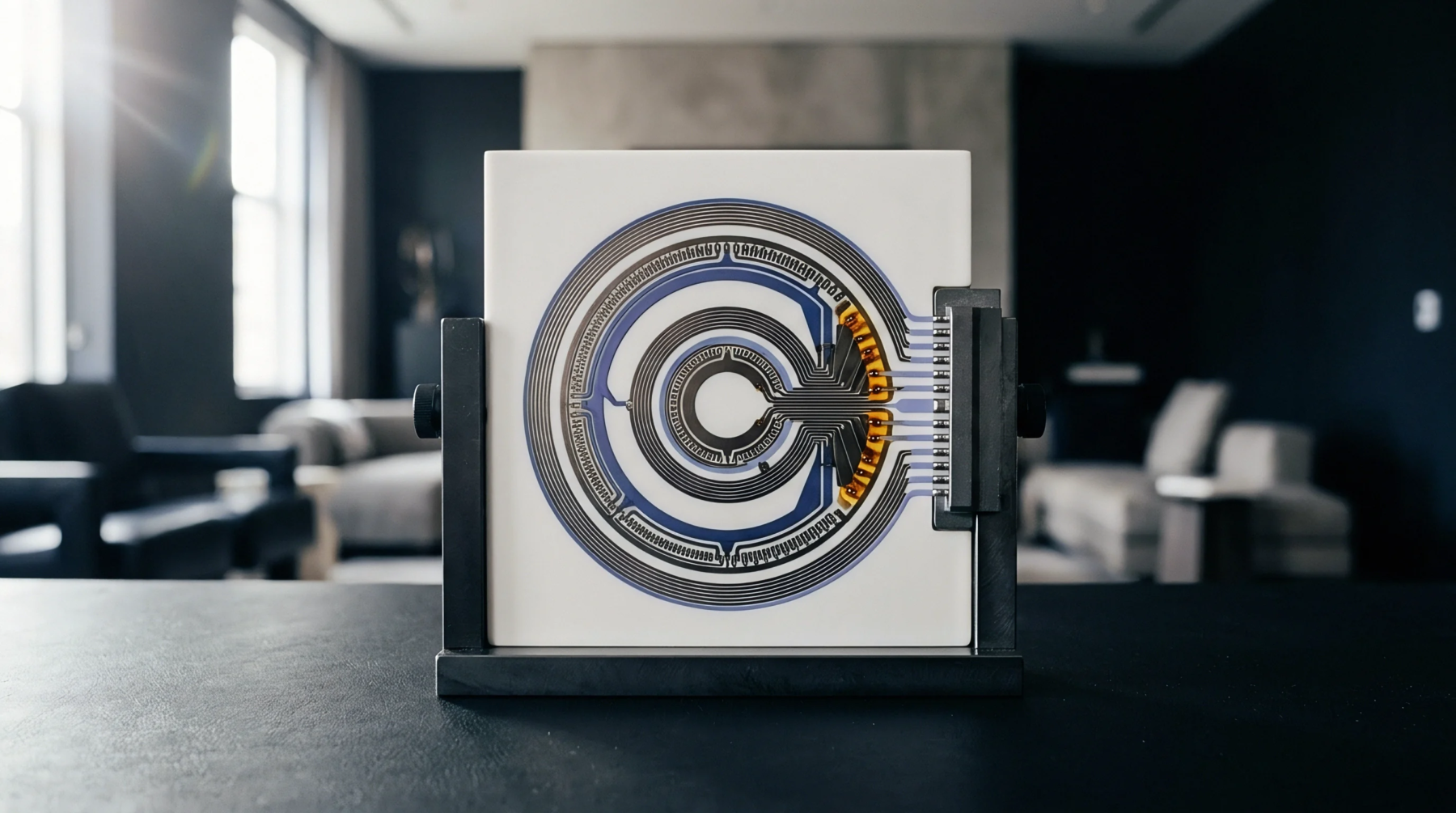
Layout configuration intended to conduct heat away from high power semiconductor devices into the internal copper layers of a circuit board defines the thermal management capability of an assembly. Proper thermal pad design balances the need for maximum metal contact with the constraints of the assembly process. This feature is often found on the underside of power regulators.
Via Integration
Small holes known as thermal vias are placed within the pad area to connect the surface copper to large planes. Through an optimized thermal pad design, these vias act as conduits for both heat and (potentially) solder wicking. Capping or filling these vias prevents the solder from draining to the back of the board.
Solderability Factor
Large solid copper areas act as heat sinks that can pull energy away from the joint during the soldering process. If the thermal pad design does not include thermal relief for surrounding connections, the local temperature may not reach the required liquidus point. This results in poor wetting or weak mechanical bonds.
Designers must calculate the total copper area to ensure the reflow profile can accommodate the thermal mass. Automated inspection often flags these areas for insufficient solder if the heat sink effect is too strong. Adding a solder mask grid on top of the pad can help control the spread of the alloy.
Consistent heating is the goal of a successful layout.