Dimensional Tolerance
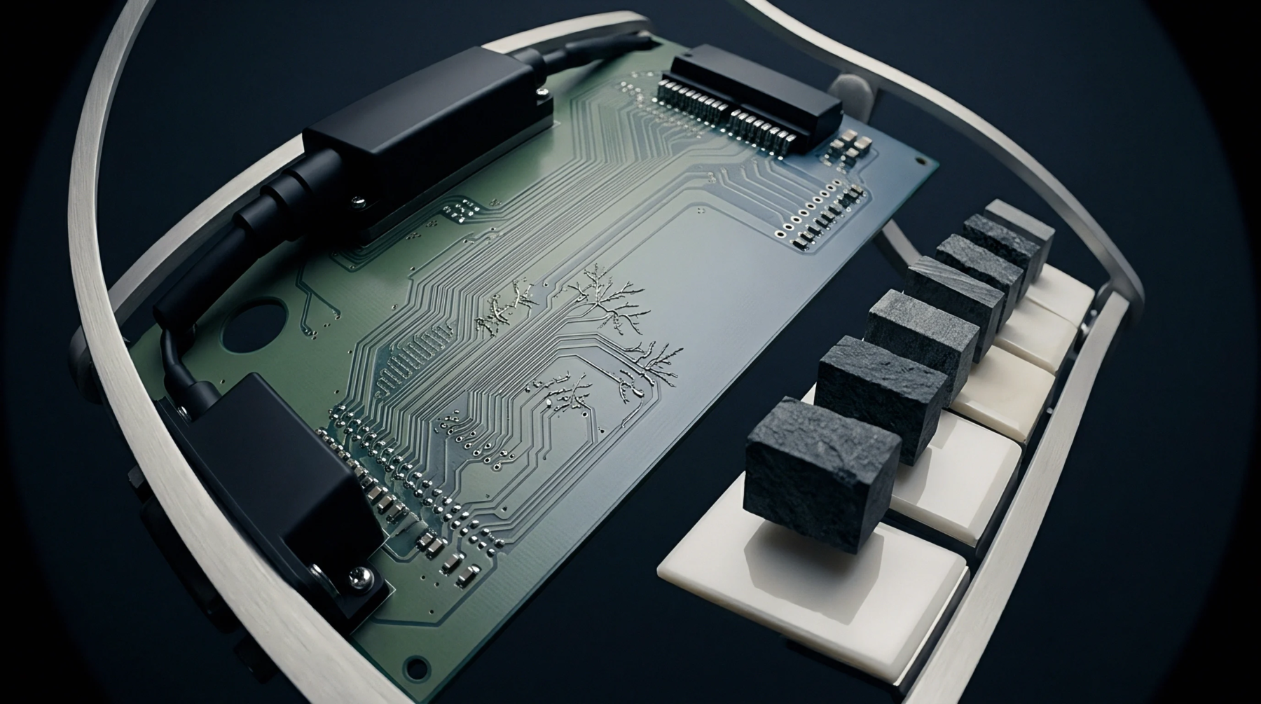
Fabrication discipline manages the physical dimensions of copper conductors on a printed circuit board to ensure they meet the electrical requirements of the design. Precise trace geometry control involves monitoring the width, thickness, spacing and cross-sectional shape of the signal lines during the etching process. Strict dimensional oversight is essential for maintaining the target impedance across a production lot.
Etch Precision
Variation in the chemical etching rate can cause traces to be narrower at the top than at the bottom, creating a trapezoidal cross-section. If the etch factor is not tightly controlled, the capacitance to the reference plane changes and alters the characteristic impedance of the circuit. Photo-imageable solder masks and high-resolution imaging equipment help to minimize these deviations.
Automated optical inspection systems measure the trace widths at multiple points on the panel to verify compliance with the design rules. Even a ten percent deviation in width leads to a significant increase in signal reflections.
Impedance Stability
Surface roughness of the copper foil also impacts the effective geometry at high frequencies. Skin effect forces the current to travel along the outer edges of the conductor where the texture of the metal increases the resistive loss. Final acceptance of the board depends on the ability of the manufacturer to hold these dimensions within the specified microns.