Interlaminar Delamination Detection Methods for High Density Interconnect Printed Circuits
Acoustic phase-inversion scanning detects latent interlaminar delamination in HDI circuits before thermal reflow turns unbonded interfaces into open circuits.


Split
Flying probe test heads register zero resistance deviation across a twelve-layer board containing fifty-micron dielectric films right up to final packaging. Continuity fixtures record clean milliohm readings across every microvia chain. Yet when passed through convection reflow at two hundred sixty degrees Celsius, the inner layers pull apart.
Copper target pads separate from adjacent dielectric surfaces as entrapped moisture expands inside microscopic unbonded boundaries. Initial electrical checks pass every panel because physical contact remains intact under mechanical clamping at room temperature. An unbonded interface continues to conduct electricity until thermal stress pulls the copper barrel away from the inner capture land.
Modern build-up architectures combine alternating strata of reinforced glass-epoxy cores and thin resin dielectric films. Blind microvias formed by ultraviolet lasers terminate on internal copper planes with target pad diameters under one hundred fifty micrometers. Adhesion between these dissimilar materials depends on surface chemical bonding, micro-roughness topography, and complete resin cross-linking.
When any parameter drifts during sequential lamination cycles, mechanical cleavage develops along the plane of weakest adhesion.
The origins of structural failure within sequential build-up layers follow specific chemical and physical pathways:
- Resin Cure Deficit results from uneven thermal distribution across multi-opening vacuum presses, leaving under-cured polymer zones with depressed glass transition temperatures.
- Silane Coupling Failure develops when organosilane adhesion promoters degrade during prolonged prepreg storage or under high relative humidity prior to lay-up.
- Oxide Conversion Breakdown appears along copper foil treatments when chemical baths lose replenishment balance, producing brittle organometallic films that fracture under shear.
- Desmear Chemistry Entrapment occurs when aggressive permanganate or plasma residue remains inside microvia cavities, eroding the bond between target pads and succeeding dielectric layers.
A six-layer HDI board undergoing three successive build-up cycles experiences multiple thermal excursions during vacuum lamination, microvia metallization, planarization grinding, and post-bake browning. Each lamination cycle subjects earlier interfaces to renewed hydrostatic pressure and temperature ramps. Internal stresses accumulate at copper-dielectric boundaries, creating localized shear fields that concentrate at the corners of filled copper vias, where thermal expansion mismatches between pure copper and unreinforced resin reach fivefold magnitude.
Standard electrical testing catches open circuits and dead shorts, but latent delamination escapes it entirely. An unbonded boundary conducts current without impediment as long as physical contact persists. Spotting it requires methods capable of interrogating internal interfaces through wave propagation, thermal diffusion anomalies, or controlled thermal stress before assembly operations commence.
Post-reflow microvia separation can stem from customer assembly profiles or lamination process drift.


Echo
Acoustic microscopy sends high-frequency mechanical sound waves directly into multilayer panels to evaluate interfacial integrity. Immersion transducers generate longitudinal pressure waves that traverse composite strata. When the advancing acoustic wave strikes an internal boundary between two distinct media, part of the wave reflects back toward the transducer while the rest transmits deeper into the structure.

Does Acoustic Impedance Mismatch Reveal Subsurface Separation?
Reflection behavior depends on the acoustic impedance difference between adjacent materials. Acoustic impedance equals material density multiplied by sound velocity within that medium. Electrodeposited copper exhibits an impedance near forty-one megarayls, whereas dielectric build-up resin sits near three megarayls.
An intact copper-to-resin interface yields a predictable reflection coefficient. Air, by contrast, has an acoustic impedance of four ten-thousandths of a megarayl, making an air-filled gap from interlaminar separation an almost complete mismatch against adjacent solid layers.
Acoustic reflection at an unbonded interface produces a 180-degree phase inversion with reflection amplitude approaching ninety-nine percent when air thickness exceeds ten nanometers.
The phase angle of the reflected waveform confirms whether a boundary meets solid material or an empty void. Reflection at an interface entering a medium of lower acoustic impedance flips the phase by one hundred eighty degrees. Transducer electronics track this phase inversion alongside signal amplitude: an intact interface reflects a positive peak when the deeper layer possesses higher impedance, while a separated boundary returns an inverted negative peak with maximum amplitude because air reflects ninety-nine percent of incident acoustic energy back to the receiver.
| Frequency | Focal Length | Spot Diameter | Penetration Limit | Minimum Detectable Separation |
|---|---|---|---|---|
| 50 MHz | 12.7 mm | 110 µm | 18.0 mm | 45 µm |
| 100 MHz | 8.0 mm | 52 µm | 6.0 mm | 20 µm |
| 175 MHz | 5.0 mm | 30 µm | 2.5 mm | 8 µm |
| 230 MHz | 4.2 mm | 18 µm | 1.2 mm | 3 µm |
| 300 MHz | 3.0 mm | 12 µm | 0.6 mm | 1 µm |
Operating frequency sets the balance between penetration depth and spatial resolution. High-density circuitry demands transducer frequencies between one hundred seventy-five and three hundred megahertz. At two hundred thirty megahertz, acoustic spot size shrinks to eighteen micrometers, allowing resolution of microvia pads and narrow signal traces.
Because sound attenuation increases with the square of frequency, ultra-thin dielectric layers of twenty-five to forty micrometers require tight electronic gating to isolate reflections of interest from surface echoes.
Water serves as the acoustic coupling medium between the piezoelectric lens and the panel surface. Traditional immersion systems submerge panels in deionized tanks, which introduces moisture absorption risks into hygroscopic dielectric materials. Scanners utilize localized water-path nozzles to maintain a continuous meniscus over the inspection zone while keeping the broader panel dry.
High scanning speeds of five hundred millimeters per second across flat panels enable rapid mapping of multi-up production arrays.
Acoustic shadow effects limit inspection beneath solid copper ground planes. Dense outer copper foil reflects sixty percent of incident acoustic energy, attenuating the pulse before it reaches deep buried microvias. Advanced signal processing relies on frequency-domain deconvolution to isolate weak echoes originating beneath dense metal patterns.

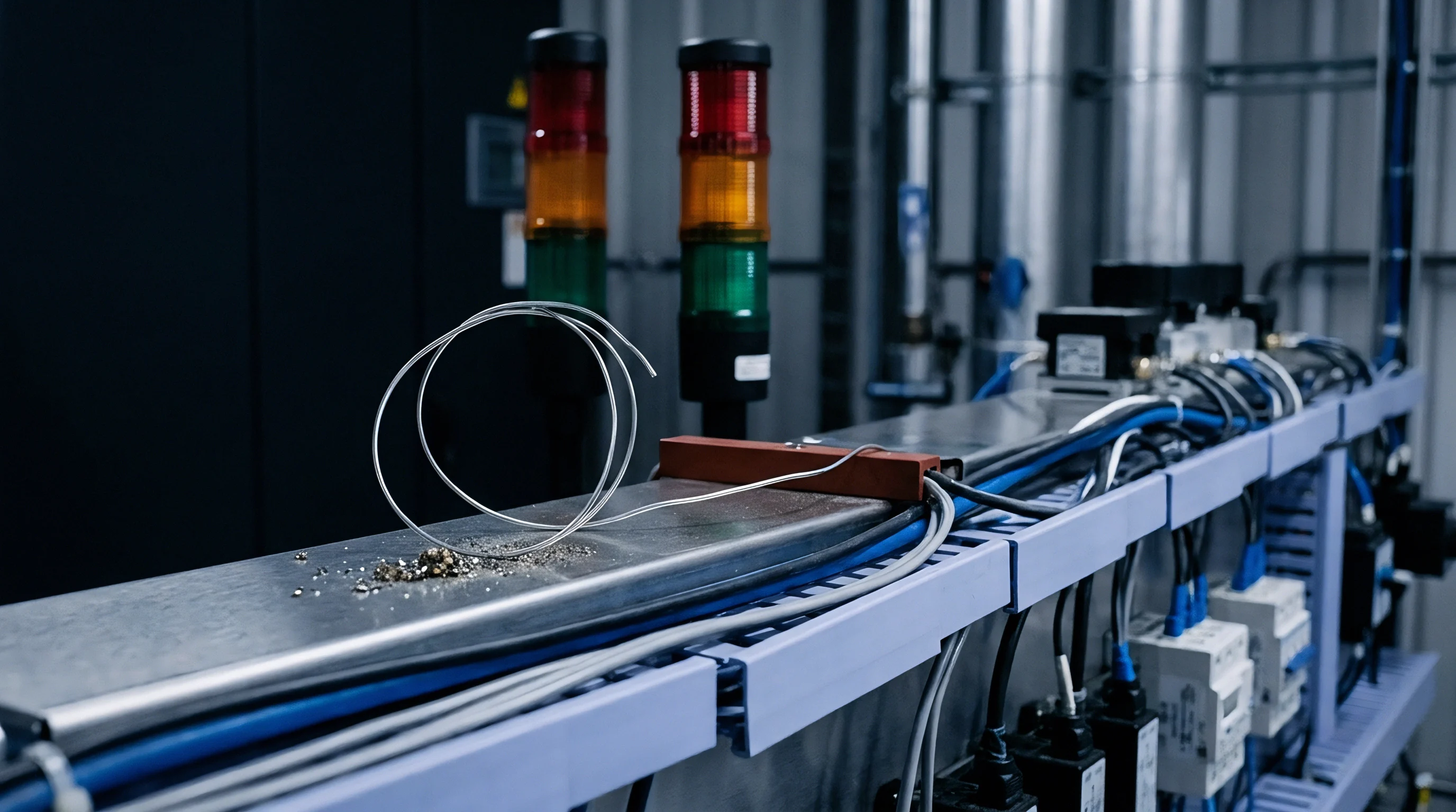
Heat
Thermal energy propagation provides another non-destructive avenue for uncovering subsurface defects. Flash thermography applies a short pulse of radiant energy to the panel surface using high-output xenon flash lamps. The surface absorbs this pulse and conducts heat inward toward inner dielectric and copper strata, while infrared cameras monitor the resulting surface temperature decay over time.
Where Does Thermal Resistance Expose Dielectric Voids?
Internal voids present severe barriers to conductive heat transfer. Air has a thermal conductivity of twenty-six thousandths of a watt per meter-Kelvin, compared to roughly three tenths of a watt per meter-Kelvin for unreinforced build-up films and four hundred watts per meter-Kelvin for copper. Heat traveling downward from the illuminated surface stalls upon encountering an unbonded zone, accumulating in the material directly above the flaw and producing a localized warm spot on the top surface.
Thinner dielectric cores transfer heat rapidly enough that surface thermal anomalies decay before focal-plane arrays register the peak temperature differential.
Infrared detectors operating in the mid-wave band capture transient temperature profiles at frame rates exceeding one kilohertz. Logarithmic derivative analysis of surface temperature curves separates depth information from surface emissivity variations. Sound laminate exhibits uniform cooling following an initial plateau, whereas laminate containing an interlaminar void displays a distinct deviation in its cooling rate slope.
The time elapsed between the flash pulse and the peak temperature contrast correlates directly with defect depth.
Thermal wave diffusion in composite circuit materials behaves identically to transient heat conduction in space-bound instrumentation housings, where layered insulating blankets reveal unbonded honeycomb skins under flash radiometry. Both systems rely on Fourier heat equations governing boundary resistance across solid-gas junctions.
| Regime | Stress Profile | Test Category | Inspection Mechanism | Defect Resolution |
|---|---|---|---|---|
| Pulsed Thermography | 5 ms optical flash, 10 J/cm² | Non-destructive | Mid-wave infrared thermography | Planar area over 100 µm |
| Lock-in Thermography | 0.5 to 10 Hz modulated heat | Non-destructive | Phase-locked radiometry | Planar area over 40 µm |
| TMA Delamination | Isothermal 260°C or 288°C | Destructive | Dimensional expansion drift | Whole-coupon bulk event |
| Solder Float | 288°C bath, 10 s floats | Destructive | Visual and microsection | Localized gross separation |
| Convection Preconditioning | 6x 260°C reflow cycles | Stressed Coupon | Interconnected resistance drift | Microvia interface tear |
Active thermographic screening operates without liquid immersion tanks, eliminating moisture contamination during in-line production testing. The method struggles, however, to resolve voids smaller than their burial depth. A delamination boundary measuring twenty micrometers across, buried seventy micrometers beneath surface copper, diffuses its thermal footprint laterally before reaching the surface, leaving temperature variations too faint to distinguish from noise.
Lock-in thermography overcomes signal-to-noise limitations by applying periodic sinusoidal heating. Modulating the excitation source at frequencies from one-half hertz to five hertz concentrates energy at specific depth planes. Phase angle imagery extracted from lock-in sequences eliminates surface reflection artefacts, revealing weak subsurface anomalies without destructively stressing the polymer chain.
Whether transient infrared screening can reliably separate nanoscale interfacial micro-voids from normal copper trace topography across five-micrometer trace widths remains an engineering dispute between panel fabricators and test houses.


Cut
Physical verification demands cross-sectional examination to arbitrate ambiguous non-destructive signals. Destructive physical analysis exposes inner strata directly to optical and electron beams. When acoustic or thermal inspections identify potential anomalies, metallographic preparation reveals the exact physical condition of copper-dielectric interfaces.

Specimen Preparation Protocol
Preserving fragile interlaminar boundaries during metallurgical preparation requires controlled cutting, mounting, grinding, and polishing stages:
- Precision diamond wheel saws isolate coupon targets using kerosene coolant at blade speeds below two thousand revolutions per minute to prevent frictional heating.
- Specimens receive vacuum impregnation within low-viscosity room-temperature curing epoxies, preventing mechanical edge pullout during material abrasion.
- Successive silicon carbide papers from three hundred twenty grit to twelve hundred grit abrade the specimen surface under thirty kilopascals of planar pressure.
- Synthetic nap cloths charged with polycrystalline diamond suspensions down to one micrometer remove mechanical scratches without rounding copper features.
- Final polishing with five-hundredths-micrometer colloidal silica suspension operating at pH nine planarizes the dielectric-copper junction.
- Light microetching using ammonium persulfate reveals the copper grain microstructure and clean interfacial boundary lines.
Field emission scanning electron microscopy inspects the polished junction at magnifications exceeding five thousand diameters. Secondary electron detectors resolve micro-cleavages below fifty nanometers along the target pad perimeter. Backscattered electron imaging maps atomic number contrast, distinguishing pure copper metallization from residual oxide films, resin matrices, and particulate contaminants.
IPC-6012 Class 3 permits zero interlaminar separation across thermal stress coupons evaluated under microsection inspection.
Energy dispersive X-ray spectroscopy identifies chemical foreign matter at the separation interface. Detecting chlorine, sulfur, or sodium inside an unbonded microvia cavity confirms chemical entrapment from etching or desmear operations. A clean separation showing no chemical residues points instead to mechanical shear failure from mismatched thermal expansion coefficients or press temperature deficits.
High-resolution three-dimensional X-ray computed micro-tomography provides volumetric reconstructions without physical cutting. Modern nanofocus X-ray tubes achieve spatial voxel resolutions down to three hundred nanometers, visualizing microvia barrels, target pads, and internal air gaps directly within intact test coupons. Because contrast differences between build-up resin and microscopic air voids remain modest, rendering fine cracks accurately requires longer exposure times and phase-contrast processing algorithms.
Under IPC-TM-650 Method 2.1.1, coupon cross-sections exhibiting any resin separation extending across more than eight percent of the distance between adjacent conductive features fail Class 3 acceptance unconditionally.

Dispute
Procurement contracts balance screening costs against the financial exposure of assembly line failure. High-density interconnect panels for aerospace, medical, and compute infrastructure carry assembly bills of materials twenty times the bare board fabrication price. An undetected interlaminar separation that survives reflow escapes into field operation, where thermal cycling turns a latent micro-separation into an open circuit.
Replacing a failed multi-chip module board in service exceeds the bare board fabrication cost by orders of magnitude.
Coupon-based lot release represents the baseline in high-volume purchasing agreements. Fabricators place test coupons containing daisy-chained microvias and solid planes along the perimeter breakaways of production panels. These coupons undergo thermal stress screening per IPC-TM-650 Method 2.4.13, followed by microsection analysis.
Perimeter coupons reflect conditions at platen edges rather than the panel center. Because multi-opening vacuum presses develop thermal and pressure gradients between peripheral borders and the center core, edge coupons frequently pass physical evaluation while panel centers suffer under-cure or resin starvation.
| Regime | Cycle Time per Panel | Unit Cost | Defect Escape Rate | Interrogated Area |
|---|---|---|---|---|
| Coupon Microsectioning | 4.0 hours per batch | $120 per section | 8.5% to 14.0% | Breakaway coupon edges only |
| Full-Panel Acoustic SAM | 3.5 minutes per panel | $8.50 per panel | 0.2% to 0.5% | 100% active board area |
| In-Line Pulsed Thermography | 12 seconds per panel | $1.10 per panel | 2.0% to 4.5% | 100% active board area |
| X-Ray Micro-CT Coupon | 45 minutes per coupon | $250 per scan | 6.0% to 11.0% | Isolated 5 mm cube target |
Production batch release documentation requires specific objective evidence to confirm lamination integrity across the whole surface:
- Thermal Expansion Logs verifying glass transition temperatures and decomposition points per lot through thermomechanical analysis curves.
- Reflow Preconditioning Records demonstrating zero resistance deviation across daisy-chains following six consecutive convective reflow passes at peak profile temperature.
- C-SAM Amplitude C-Scans documenting the entire panel active area with gated reflection imagery confirming absence of phase-inverted acoustic returns.
- Platen Temperature Telemetry recording thermocouple data across center and corner zones for every lamination press press-cycle.
A typical scenario clarifies the economic arithmetic. Assume a production batch of two thousand ten-layer HDI panels destined for mission-critical networking hardware, with bare panels valued at eighty dollars each and fully loaded assemblies valued at eighteen hundred dollars. Relying exclusively on edge coupon microsections leaves an escape rate of approximately eight percent for center-panel delamination events under uneven press heat.
That escape rate translates into one hundred sixty defective assemblies passing through component placement and soldering. Component loss and assembly labor push scrap costs to two hundred eighty-eight thousand dollars, not counting diagnostic delays.
Implementing one hundred percent scanning acoustic microscopy on bare panels adds seventeen thousand dollars in screening fees across the lot. Acoustic inspection identifies latent unbonded areas immediately, rejecting defective panels before surface mount placement consumes expensive processors. Yield drops at bare board acceptance, but scrap costs at the loaded board level disappear entirely.
Coupons placed along panel breakaways document edge lamination conditions while missing resin starvation at the panel center.
Buyers who accept certificates of conformance without demanding full acoustic scan files or destructive center-panel evaluations bear the full replacement cost when thermal stress tears internal interfaces apart in the field.