Microscopic footprint dimensions
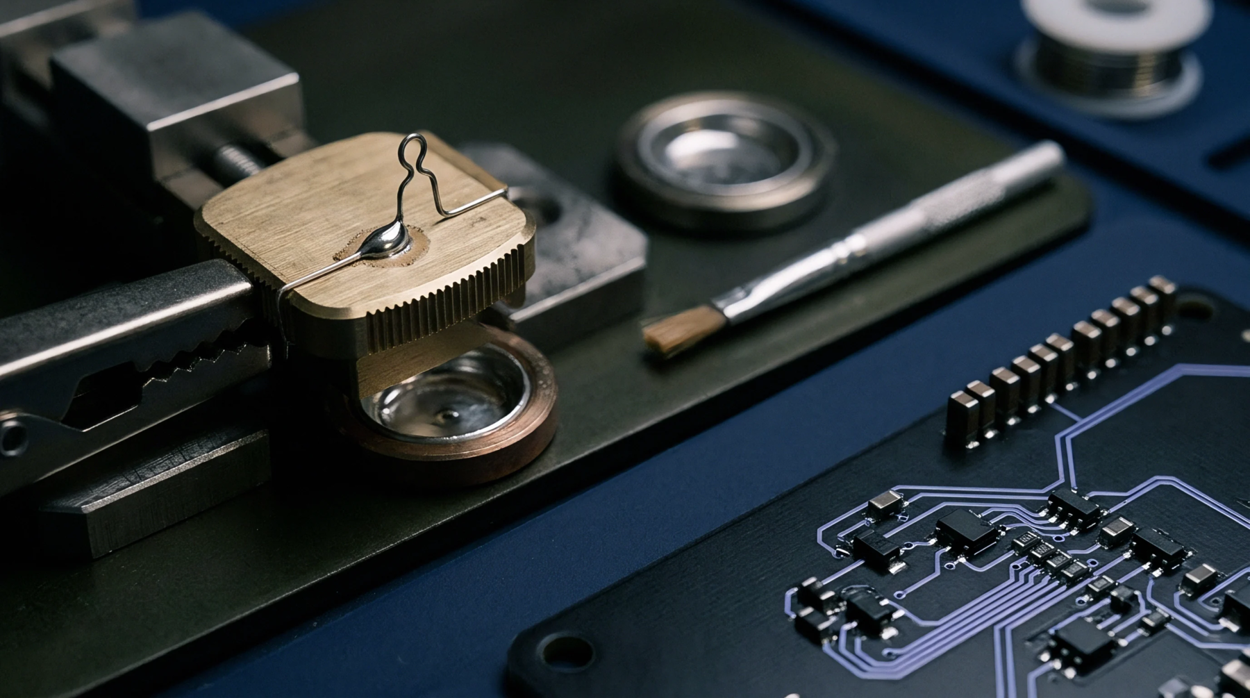
Metric sizing defines the 008004 components by their nominal length and width of point two millimeters by zero point one millimeters. These passive elements represent the smallest surface mount technology standard currently utilized in high density circuit board population. Physical miniaturization dictates specialized handling equipment because the parts possess insufficient surface area for conventional mechanical vacuum nozzles.
Operators utilize high resolution optical alignment systems during the pick and place operation to ensure accurate placement on solder paste deposits.
Tolerance constraint
Manufacturing specifications for these tiny parts demand extreme precision in pad geometry and paste volume control. Variability in stencil thickness or aperture shape creates immediate issues with tombstoning or bridging during the reflow heating cycle. Engineers specify laser cut stainless steel stencils with electropolished walls to minimize friction during paste release onto the copper pads.
Tight control over the board surface finish further dictates the success of the soldering process for such restricted landing zones.
Assembly reliability
Thermal cycling tests verify the robustness of solder joints formed by 008004 components when subjected to standard electronics operation conditions. Mechanical stress at the substrate interface becomes the limiting factor for bond integrity because the absolute amount of solder alloy is minimal. Careful optimization of the reflow temperature profile prevents both cold joints and intermetallic compound overgrowth which compromises electrical conductivity over the projected life of the circuit.
Long term connection stability depends entirely on the accuracy of the initial alignment and the uniformity of the heating distribution across the assembly.