Geometric Verification
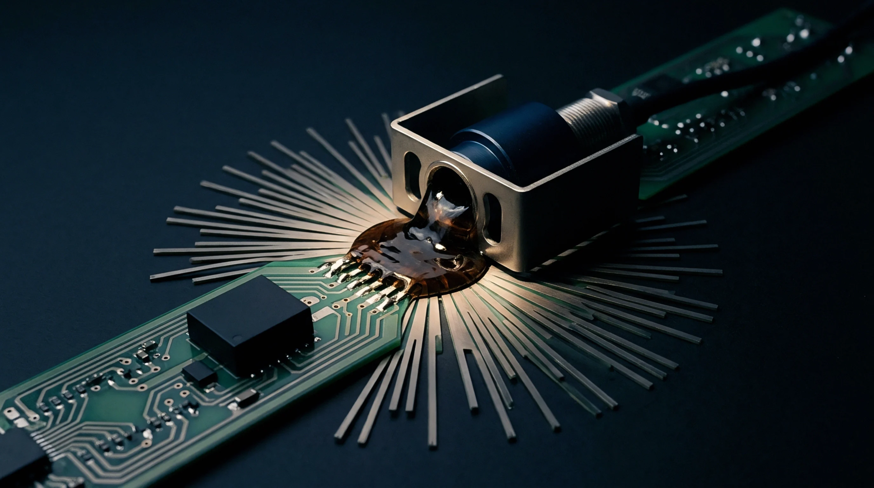
Dimensional analysis establishes the fidelity of high density interconnects during the assembly of heterogeneous semiconductor systems. Advanced packaging metrology provides the measurement capability required to map the coplanarity and registration of components that possess sub-micron features. Integrated circuits often undergo structural deformation during the thermal cycling inherent to solder reflow processes.
Sensor arrays detect these topographical shifts by quantifying the warpage of substrate surfaces against ideal geometric planes. Data collected during these inspections determine the pass or fail status of individual units prior to the application of expensive encapsulation materials.
Systematic Correlation
Statistical feedback from the production line validates the alignment of silicon dies within multi-chip modules. Advanced packaging metrology captures the vertical profile of bumps and pillars to predict the reliability of electrical contact points. Automated optical inspection tools record the X-ray diffraction patterns of internal structures to identify latent voids or cracks in the underfill layer.
Discrepancies in the height of micro-bumps beyond defined tolerances trigger a rejection of the assembly to prevent short circuits in operation. Process engineers utilize these findings to adjust laser drilling parameters or bonding force settings on the assembly tool.
Measurement Boundary
Spatial constraints limit the resolution of inspection equipment when evaluating structures smaller than one micron. Advanced packaging metrology reaches the physical threshold of light diffraction which necessitates the adoption of scanning electron microscopy for characterization. Non-destructive techniques remain preferred for production environments whereas destructive cross sectioning serves as a method for root cause analysis during failure investigations.
Physical measurement of feature geometry remains limited by the accessibility of hidden interfaces inside stacked die configurations. These limitations restrict the verification process to exterior features or specific internal layers reachable by high energy imaging waves. Success in modern microelectronic fabrication depends entirely on the precision of these dimensional controls.