Dielectric Characterization
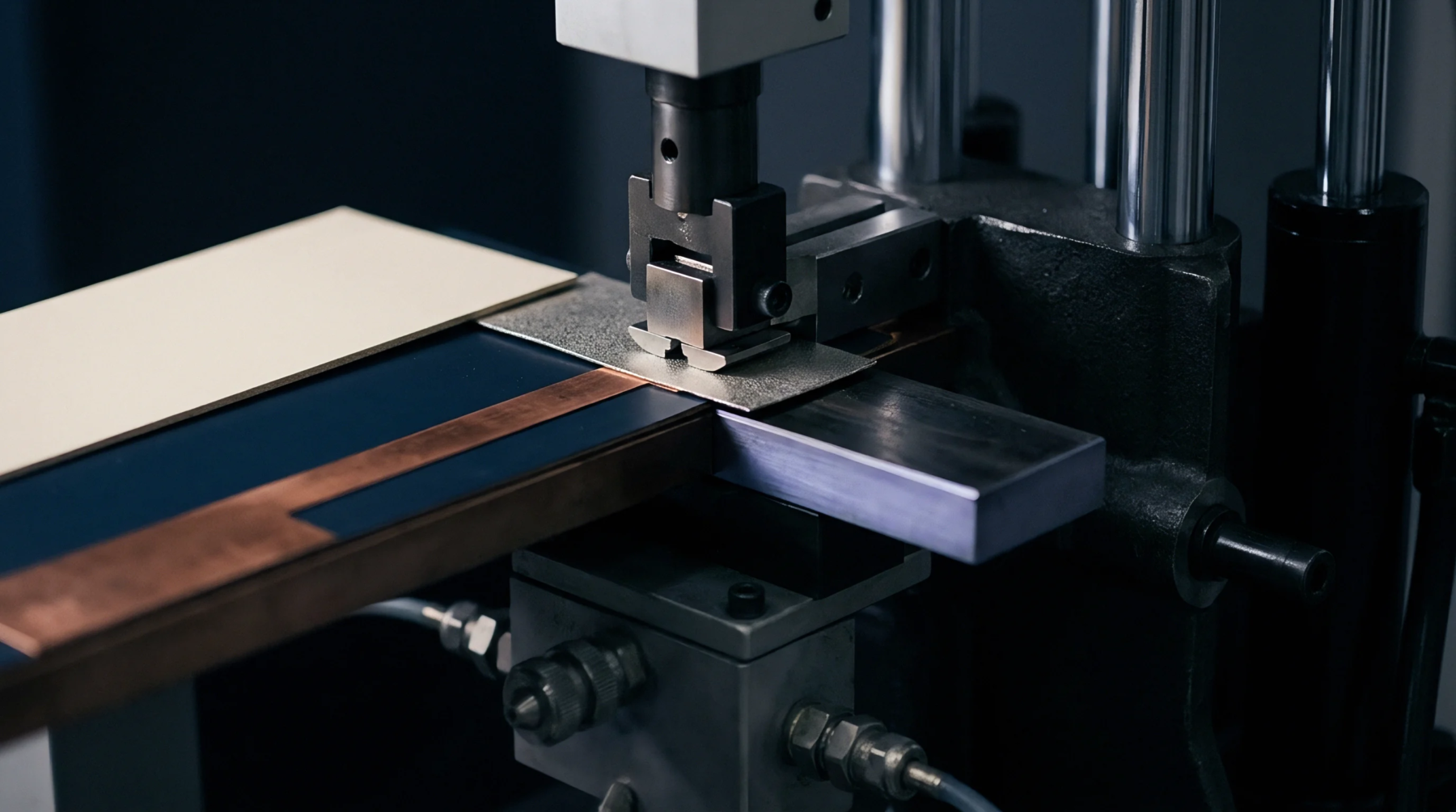
Dielectric measurement fixtures for printed circuit board laminates require high-precision compensation to account for minute mechanical gaps between the specimen and the conductor plates. This computational correction, known as air gap de-embedding, extracts the true permittivity and loss tangent of the substrate material by mathematically subtracting the capacitive contribution of the intervening air layer. Without this step, even a micrometric gap leads to a severe underestimation of the dielectric constant during high-frequency material testing.
Mathematical Adjustment
Calculating the corrected dielectric constant relies on modelling the fixture as two series-connected capacitors representing the air gap and the sample itself. Standard thickness measurements of both the laminate and the gap provide the physical dimensions for the compensation formulas. Precise thickness measurements prevent the propagation of geometric errors into the calculated electromagnetic properties of the circuit board material.
High-frequency design teams rely on these calculated values to predict trace impedance in multi-gigabit backplanes.
Permittivity Accuracy
Failure to apply this compensation results in poorly matched transmission lines on the finished printed circuit board. Circuit designs calculated with incorrect raw permittivity figures exhibit phase distortion and signal attenuation at millimeter-wave frequencies. Thus, testing laboratories must run de-embedding protocols to qualify laminate supplies before board manufacturing begins.