Trace Metrology
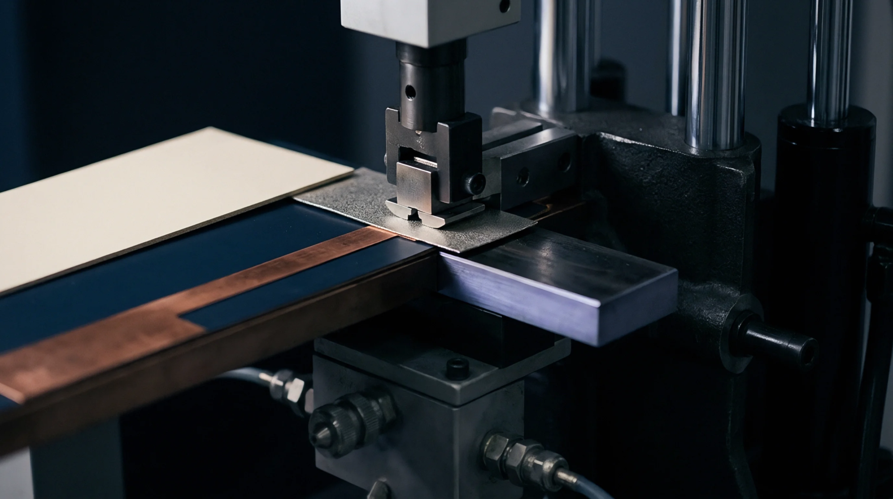
High-frequency transmission performance across printed circuit boards is evaluated using standardized sacrificial track patterns placed on panel breakout margins. Quality assurance regimes verify coupon impedance using time domain reflectometry to confirm that line geometries, dielectric spacing, and resin cure levels meet specified target values. Designers define controlled impedance tracks on production circuits, but destructive probing directly on flight boards risks mechanical damage to fine-pitch solder mask openings and fragile microvias.
Sacrificial test coupons replicate the identical copper layer stack, trace width, dielectric core thickness, and reference plane spacing of functional signal nets. A controlled pulse injected into the coupon reveals the characteristic impedance profile across the trace length. Deviations greater than ten percent from contractual targets like fifty ohms single-ended or one hundred ohms differential lead to panel lot rejection at incoming receiving inspection.
Dielectric Influence
Physical trace geometries and prepreg resin content determine whether signal paths meet impedance targets after multi-layer lamination. Variations in core thickness or resin-to-glass ratios directly alter the effective dielectric constant observed by high-speed signals. Fabricators measure coupon impedance across multiple panel locations to map cross-board uniformity during etching and pressing cycles.
Copper thinning during micro-etching processes lowers trace height, which drives characteristic impedance upward unless compensation allowances are calculated into phototooling files. Excessive lamination pressure squeezes resin out at panel borders, leaving center locations with thicker prepreg layers and different capacitive coupling characteristics. Solder mask application introduces an additional thin dielectric layer over exposed surface microstrips, depressing impedance by two to four ohms compared to bare copper measurements.
Conductor Tolerance
Conductor cross-sections exhibit trapezoidal etch profiles caused by chemical spray patterns inside horizontal conveyorized etching chambers. Etch undercut narrows the trace crest relative to its base, altering capacitive coupling to adjacent reference grounds. Fabricators use coupon impedance data to adjust chemical replenish rates and conveyor speeds during production runs, compensating for copper thickness variations across different plating baths.
Stripline geometries buried inside inner layers escape the chemical effects of subsequent outer layer processing, yet they remain vulnerable to prepreg flow inconsistency and glass weave skew. High-density interconnect designs with trace widths below seventy-five micrometres show heightened sensitivity to copper grain structure and foil roughness, requiring specialized coupon layouts with ground-shielded launch points to prevent probe pad parasitic capacitance from corrupting measurement traces.