Mechanical Strain
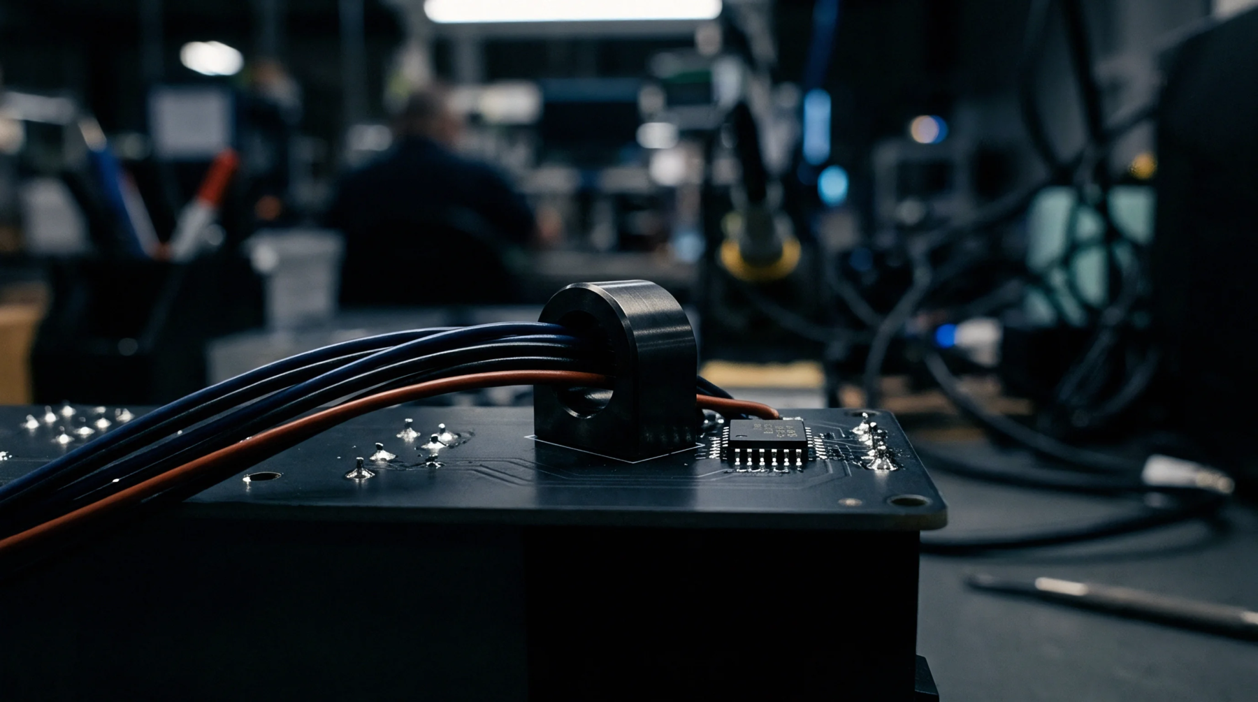
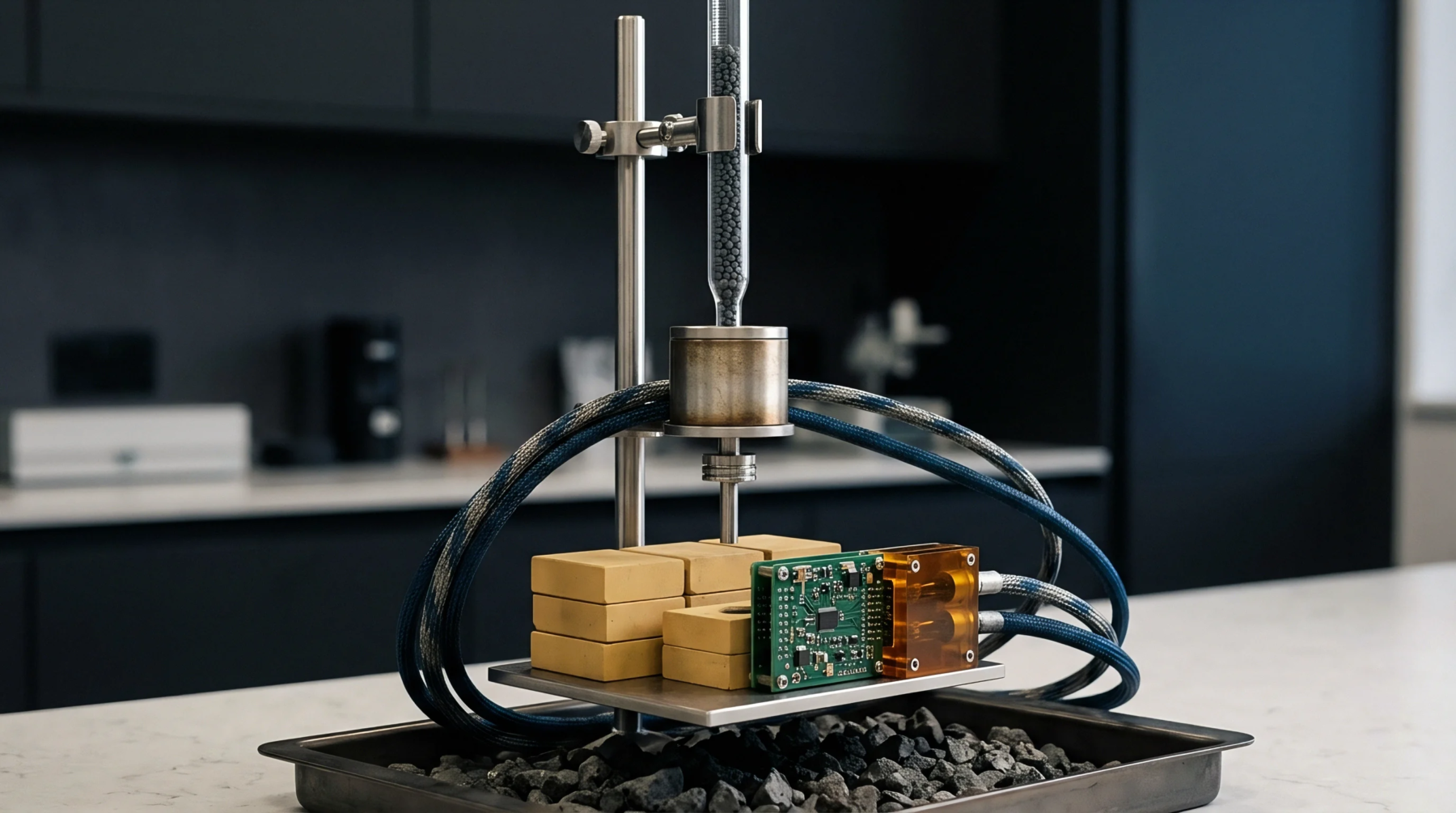
Localized strain concentrations occur where internal copper pathways run orthogonally on adjacent layers of a multilayer circuit board. This crossover stress accumulates during heat cycles due to the anisotropic thermal expansion of the composite substrate. Micro-cracks can develop in the thin dielectric layer that separates the orthogonal copper traces, leading to insulation breakdown.
Thermal Deformation
During the assembly phase, reflow temperatures exceeding 250 degrees Celsius cause the epoxy matrix to expand rapidly while the copper traces restrict motion. This differential movement creates a high concentration of shear stress at the intersection points, which is the primary source of crossover stress. If the board is subjected to rapid thermal cycling, these localized forces can cause adhesive failure between the copper and the glass-reinforced epoxy.
Boards utilizing thick copper foils or very thin prepreg layers are particularly vulnerable to this form of damage because the physical barrier between the conductors is thinner and less compliant. Designers must use solid ground planes or wider trace spacing to reduce the concentration of these internal forces.
Assembly Reliability
In-circuit testing and board inspection can reveal the electrical consequences of these high-stress intersections. Microsection analysis often shows that crossover stress produces microscopic tears in the copper foil or fractures in the surrounding resin. Measuring the change in resistance across the adjacent networks after reflow can detect these failures before the boards are shipped to customers.