Plating Anomaly
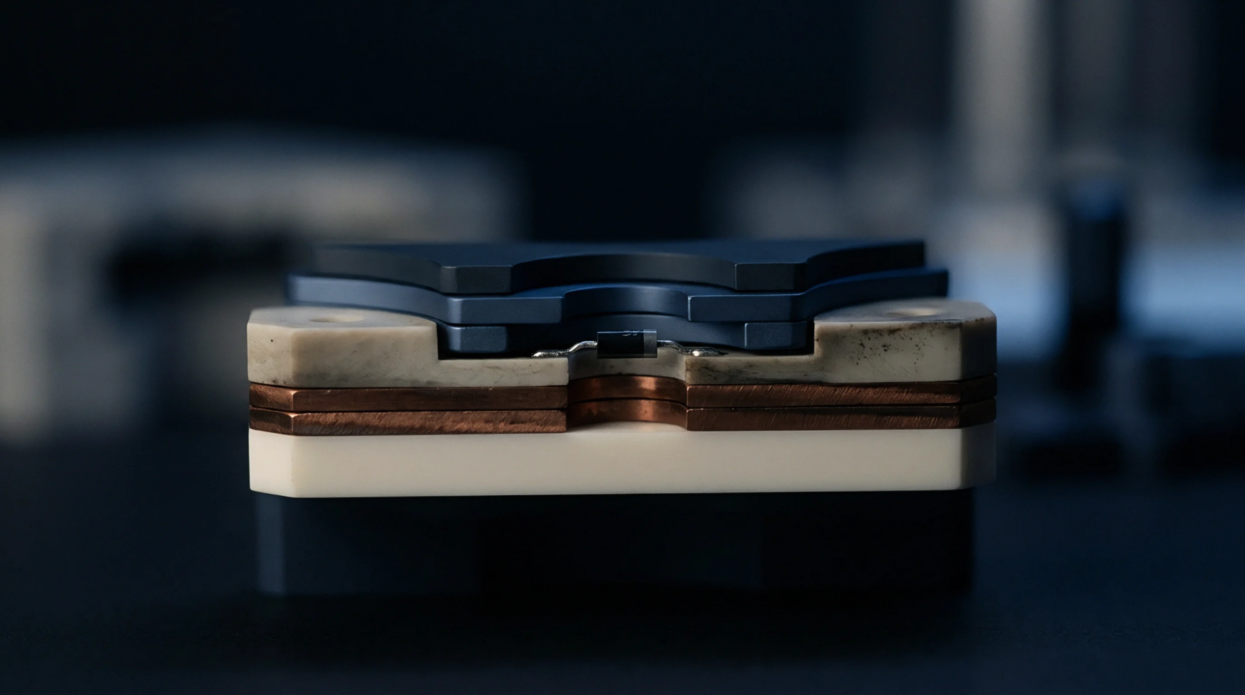
Non-uniform electrochemical copper deposition causes trace edges, isolated circuit corners, and through-hole barrel ends to develop enlarged, bulbous cross-sections. This dog boning manifests when localized current density spikes sharply at physical conductor boundaries exposed to the acid copper electrolyte. The geometry resembles a bone shape in microsection, with the conductor periphery substantially thicker than the central trace or planar field.
Acid plating baths lacking sufficient organic leveler additives produce this profile on outer-layer features. Isolated tracks facing wide, unpatterned laminate expanses suffer the greatest current accumulation. The condition alters outer-layer planarization, impedes solder mask application, and distorts downstream microstrip characteristic impedance.
Process Dynamics
Electroplating ions migrate along path lines defined by the primary electric potential field between soluble copper anodes and the cathodically biased production panel. High electric field gradients naturally congregate on sharp corners, outer trace edges, and the exposed rims of drilled through-holes. Without mass-transport leveling agents, copper ions deposit at elevated rates along these perimeter zones, starving adjacent recessed surfaces.
Severe dog boning on hole rims constricts through-hole barrel entrances before the cylinder center plates to nominal thickness, producing hour-glass hole profiles. Slower agitation rates and excessive current densities exacerbate the geometric disparity across dense versus isolated panel locations. Organic brighteners and suppressors added to the bath inhibit this preferential peripheral plating by absorbing onto high-velocity diffusion points.
Regular chemical replenishment and air or eductor agitation minimize the boundary layer variations that fuel the defect.
Assembly Defects
Raised outer trace profiles prevent planar solder mask deposition, resulting in mask thinning or complete mechanical dewetting over elevated conductor ridges. Solder bridging occurs during surface mount reflow when solder paste spreads uncontrolled across uneven pad crowns. Planar component placement tools miscalculate vertical z-axis seating heights when surface mount pads exhibit convex, bone-shaped surfaces.
Trace thickness variation across high-speed net channels introduces phase delay skew and unexpected transmission reflections. Microsections cut through drilled barrels reveal out-of-specification hole wall thickness when surface rim copper grows thick while midpoint barrel plating fails IPC minimum thickness criteria. Chemical mechanical planarization or aggressive secondary scrubbing must flatten severe conductor irregularities, risking outer-layer circuit damage.