Structural Ratio
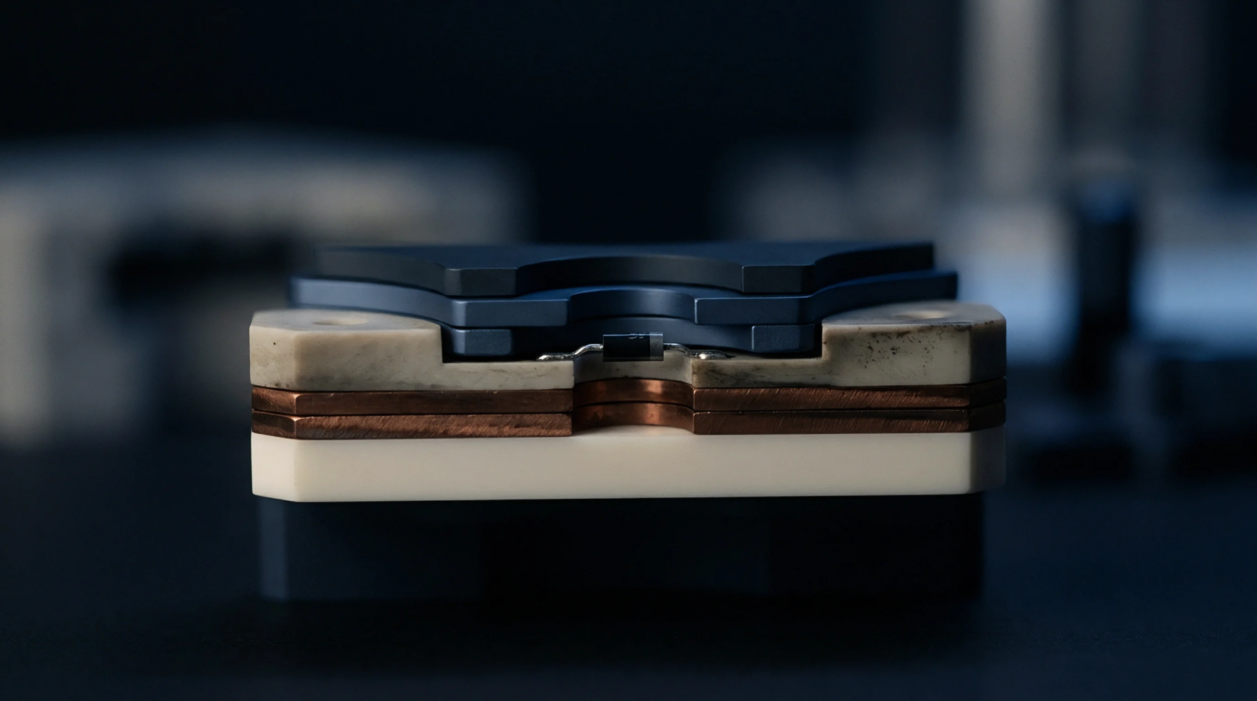
Metric calculations evaluating the distribution of metal across printed circuit board panels determine the ratio of copper area between opposing layers and across distinct surface quadrants. This panel copper balance measures the structural and galvanic symmetry of conductive patterns across inner and outer laminates throughout multi-layer manufacturing. Proper balance demands equivalent copper density on opposing layer pairs reflected about the central core axis.
Unequal distribution across panel surfaces produces structural instability, thermal twisting, and uneven plating thickness. The property is evaluated during CAM engineering preparation before releasing production photomasks or drill programs. Fabricators calculate copper coverage as a percentage per layer, striving to keep adjacent and mirror layers within five to ten percent of each other.
Warpage Prevention
Multi-layer circuit boards consist of woven glass reinforced epoxy dielectrics and copper foils that possess divergent coefficients of thermal expansion. Mismatched panel copper balance generates differential expansion and contraction forces during high-temperature prepreg lamination, solder mask curing, and automated reflow soldering. An imbalance where layer one carries ninety percent copper while layer eight carries ten percent causes severe bow and twist deformation.
SMT pick-and-place nozzles fail to seat components reliably on bowed panels, causing open solder joints and misaligned passives. Wave solder entry drags unevenly across warped boards, causing solder skips or bridging across fine-pitch leads. Symmetrical copper stacking ensures mechanical stresses counteract each other uniformly, maintaining board planarity within the zero point seven five percent bow and twist limit established by IPC-A-600.
Galvanic Uniformity
Plating current distributes unevenly across panels displaying asymmetrical copper surface areas, driving excessive copper buildup onto isolated traces while starving high-density circuit zones. A sparse quadrant draws disproportionately high cathode current density, causing trace overplating, rounded conductor tops, and severe undercut during final etching. Panel copper balance controls this dynamic by adding cross-hatched or dot matrix dummy thieving patterns into unrouted areas.
Chemical etching solutions clear balanced panels uniformly, ensuring trace width tolerances remain consistent across every circuit image on the production master. Over-etched fine tracks and unetched copper spaces on the same layer are prevented when copper mass is distributed evenly across the panel face. Solder mask cure shrinkage also proceeds symmetrically, avoiding localized stress concentrations that cause board corners to curl during cool-down.