Additive Manufacturing
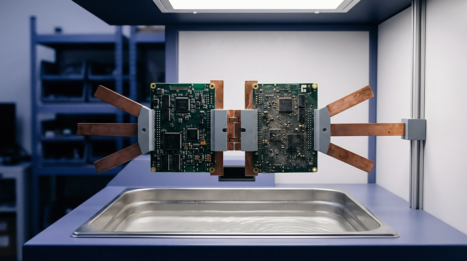
Electrolytic deposition of metal onto a patterned mandrel builds precision thin-foil components atom by atom until a structural, self-supporting metal sheet is established. The electroforming process deposits fine-grained nickel or nickel-manganese alloys onto conductive or photoresist-patterned master mandrels immersed inside an aqueous chemical electrolyte. Once the desired metal thickness is reached, the plated metal sheet is separated mechanically from the mandrel without destroying the master pattern.
This method produces solder paste printing stencils possessing aperture walls with exceptional surface smoothness and precise edge acuity. The process operates additively, eliminating the chemical undercut, thermal stress, and micro-roughness associated with subtractive etching and laser cutting. Aperture geometries down to fifty micrometers maintain straight, untapered side walls and smooth internal corners.
Paste Release
Solder paste transfer efficiency during surface mount stencil printing depends upon the contact friction between paste alloy particles and the interior aperture sidewalls. Electroformed aperture walls possess sub-micron surface roughness, exhibiting mirror-like smoothness that promotes clean, complete paste release. The ultra-smooth sidewall profile facilitates low area-ratio printing, enabling consistent paste release on apertures with area ratios dropping down to zero point five five.
Trapezoidal wall cross-sections develop naturally through photoresist mandrel profiling, presenting slightly wider exit openings on the board side than entry openings on the squeegee side. Fine-pitch ball grid arrays, wafer-level chip-scale packages, and 01005 passive components achieve repeatable solder volume deposits without bridging or paste starvation. Stencil cleaning cycles decrease in frequency because paste residues do not adhere to smooth electroformed aperture interiors.
Print definition remains stable across lengthy production runs, minimizing solder paste smearing under the foil.
Process Bounds
Fabrication cycle times for electroformed stencils extend beyond laser cutting workflows due to slow electrolytic deposition rates in chemical baths. Tooling costs are elevated because high-precision photolithography, photoresist application, and mandrel development are required before metal deposition begins. Chemical bath composition must be monitored rigorously, as slight variations in nickel sulfamate, boric acid, and organic stress-reducer concentrations cause foil brittleness or severe warping.
Stencil thickness is restricted to practical limits between twenty-five and one hundred and fifty micrometers, rendering the method unsuitable for thick-foil industrial solder applications. Mechanical damage to the ductile nickel foil during print operations cannot be repaired, demanding complete stencil replacement upon denting or creasing. Foil cost restricts the deployment of this technique to ultra-fine-pitch component assemblies where standard laser-cut stencils fail solder volume repeatability criteria.