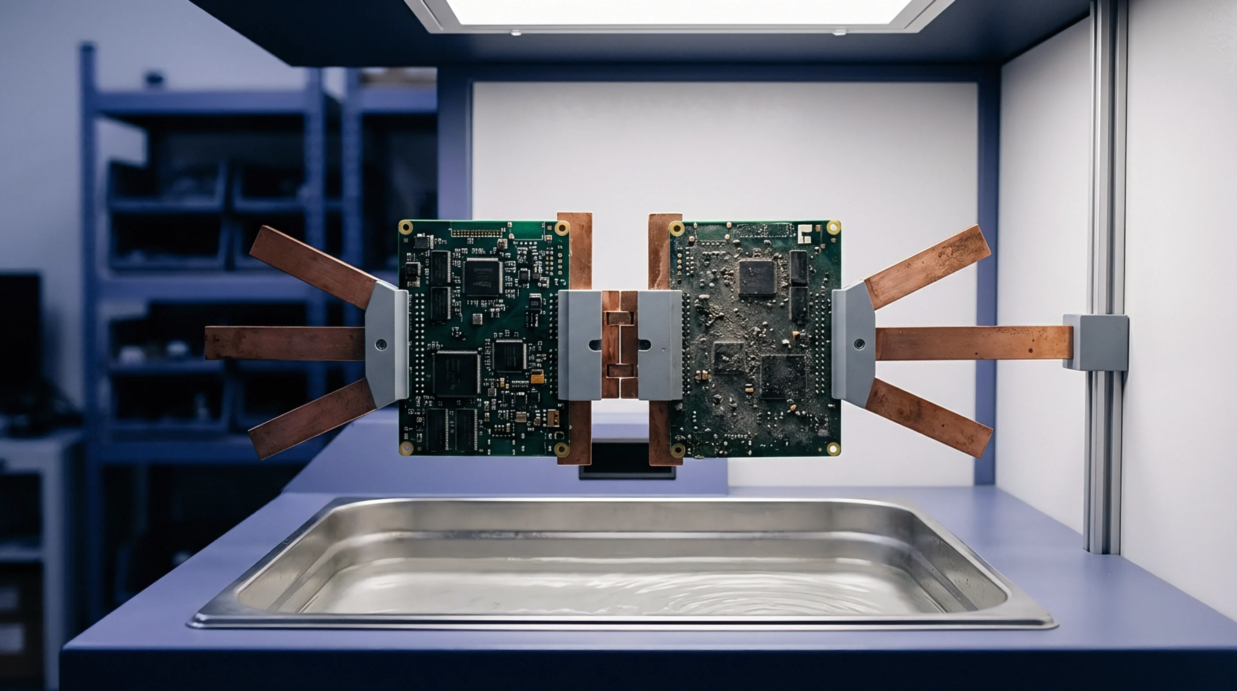
Lithographic Definition
Selective exposure of a light-sensitive polymer coating on a copper-clad laminate defines the spatial distribution of circuit traces during board fabrication. The use of photoresist patterning enables the precise creation of dense conductive pathways by shielding specific areas of the copper from subsequent etching processes. This chemical masking is the foundational step in producing high-density interconnect circuit boards.
Exposure Process
Photolithography utilizes ultraviolet light passed through a high-resolution mask to alter the solubility of the polymer layer. During photoresist patterning, the exposed areas of the polymer either harden or become soluble, depending on whether a negative or positive resist is used. The subsequent development step washes away the unhardened resist, leaving the desired copper pattern exposed for etching.
Resolution Boundary
Precision of the transfer process dictates the minimum line width and spacing that can be achieved on the finished board. Inadequate control of the exposure time or intensity in photoresist patterning can lead to under-exposure or over-exposure, resulting in trace defects such as shorts or open circuits. Consequently, maintaining tight control over cleanroom humidity, temperature, and exposure parameters is necessary to achieve the fine geometries required by modern microelectronics, ensuring that the polymer masks remain sharp and accurate across the entire surface.
This precision prevents defects before the board enters the final etching and plating stages.