Connection Geometry
Direct electrical contact between a semiconductor die and a carrier substrate occurs through conductive bumps rather than traditional wire bonds. Flip chip packaging relies on this dense array of solder balls to minimize signal paths and inductance between the integrated circuit and the printed circuit board. Smaller footprints and reduced parasitic capacitance define its utility for high speed processors and mobile hardware.
Assembly Mechanics
Placement machines align the silicon die upside down on the substrate to bring the solder bumps into contact with the landing pads. Heat reflow turns the solder into a liquid state to form the mechanical and electrical joint before cooling completes the cycle. Underside epoxy resins compensate for differences in thermal expansion rates between the silicon and the laminate carrier to prevent fatigue.
This application requires extreme precision in component orientation and temperature control across the entire heating profile. Stress concentrations often appear at the periphery of the die where the stiffness of the silicon meets the flexibility of the organic base. Designers manage these forces by adding structural reinforcements to the corners of the component.
Inspection Protocol
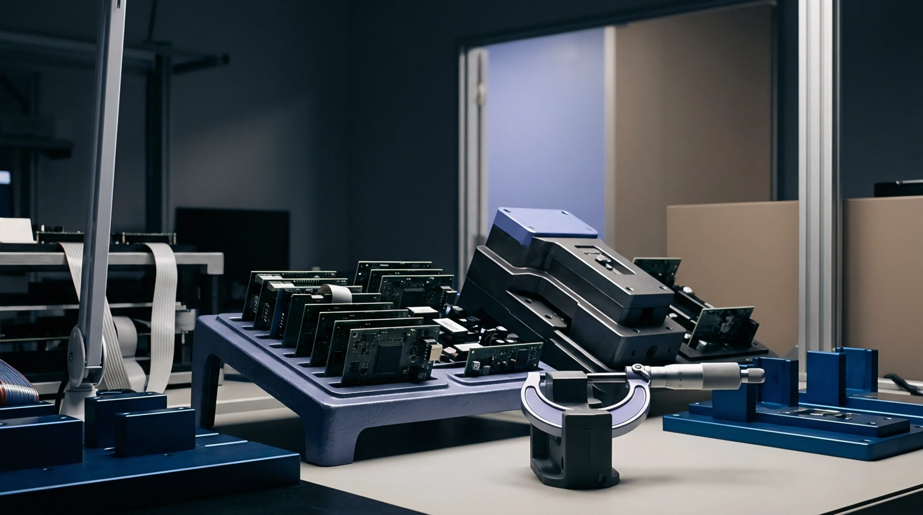
Automated optical inspection units scan the underside of the component after reflow to verify alignment and check for bridging defects. X ray imaging identifies hidden voids or open circuits within the array of solder balls that optical systems cannot see. Engineers perform shear testing on trial assemblies to quantify the force required to detach the die from the surface.
Low shear values indicate poor wetting or excessive contamination of the metallic interfaces. A properly formed joint provides sufficient mechanical strength to withstand standard thermal cycling tests without fracturing.