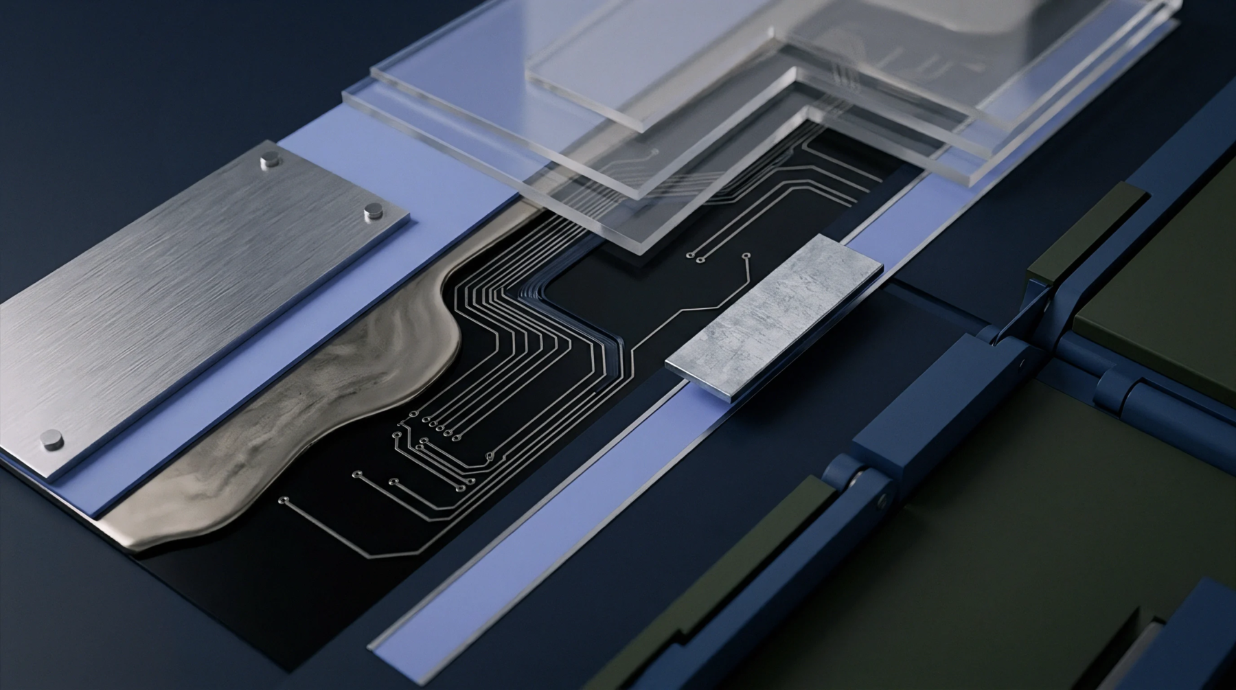
Thermal Distortion
Dynamic measurement of the flatness of an integrated circuit package occurs as the component undergoes the heating and cooling phases of a reflow profile. Package warpage tracking captures the change in coplanarity that results from mismatched coefficients of thermal expansion between the silicon, the substrate, the adhesive and the mold compound. This data helps predict whether the leads or balls will successfully contact the solder paste on the board.
Measurement Technique
Shadow moire or digital fringe projection systems project patterns onto the component surface to map its topography in three dimensions. As the temperature rises in the oven simulation chamber, the system records the transition from a flat state to a concave or convex profile. A deviation of more than 0.1 millimeters across the diagonal of a large BGA often indicates a high risk of open joints or solder bridging.
The system captures these topographic maps at specific intervals corresponding to the ramp, soak and peak temperatures of a standard assembly profile.
Consequence Path
Excessive movement during the liquidus phase of the solder can pull pins out of the molten paste or squash them into adjacent pads. If the warpage is not managed through material selection or design changes, the assembly process will suffer from low yields and hidden reliability defects. Tracking ensures that the mechanical behavior of the package remains within the tolerances of the assembly equipment.