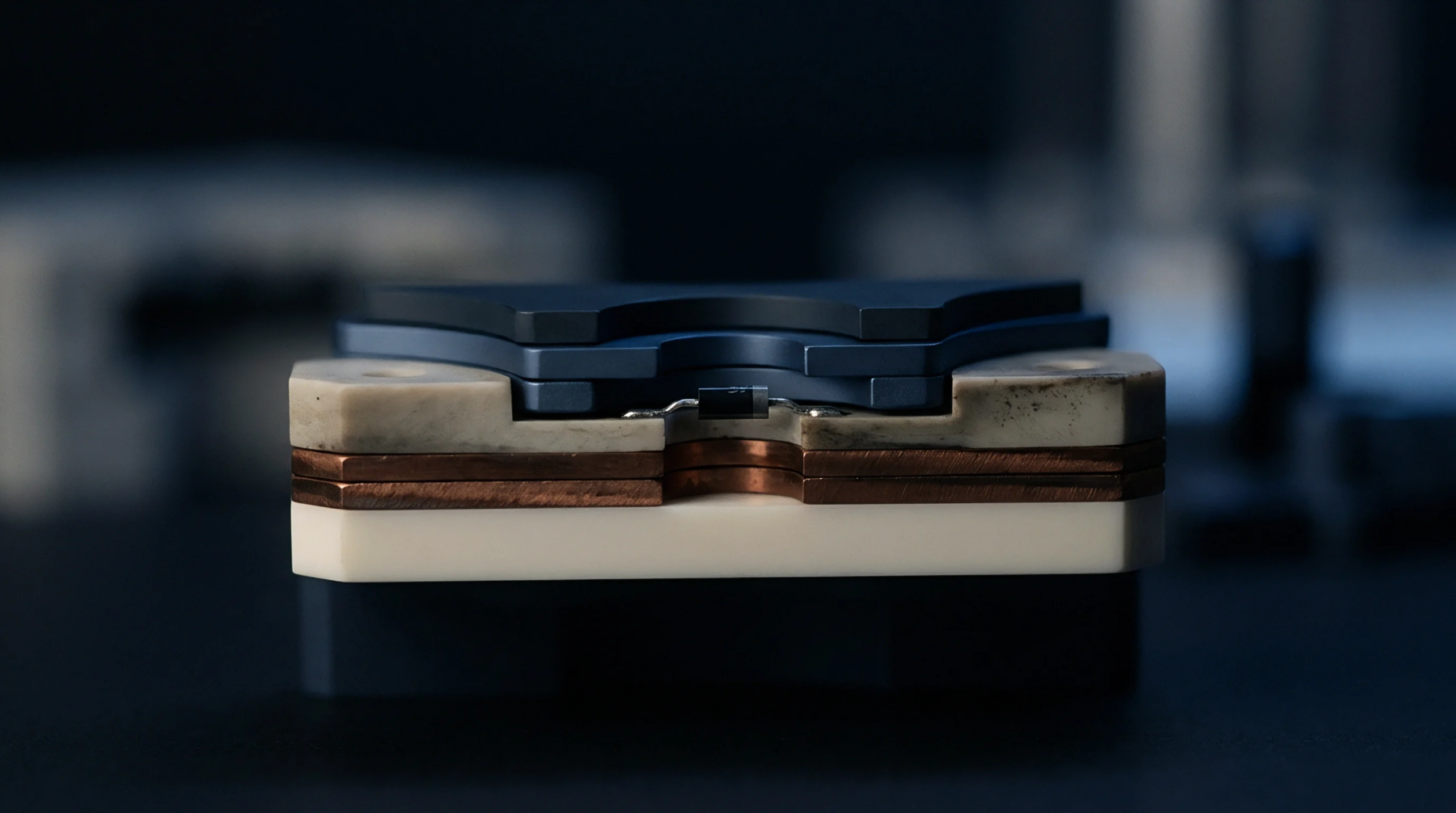
Differential Abrasion
Excessive wear on soft materials relative to hard materials during sample preparation results in a non-planar surface at material boundaries. When preparing cross-sections of circuit boards, relief polishing occurs when the softer resin or solder is worn away faster than the harder copper tracks. This non-planar finish distorts the sample, making accurate measurements of plating thickness difficult under high magnification.
Specimen Integrity
Maintaining a perfectly flat surface across diverse material hardnesses is critical for high-resolution microstructural imaging. Standard abrasive pads and high-pile polishing cloths cause relief polishing by yielding under pressure and reaching into the softer areas of the mounted sample. To prevent this, technicians use low-pile, hard-woven cloths with high concentrations of diamond paste.
This method forces the abrasive to cut uniformly across both hard and soft materials, preserving a level plane at the copper-to-resin border. It eliminates the shadow effects and optical distortion that occur during high-magnification quality checks.
Microscopic Assessment
Optical microscopes cannot focus simultaneously on two distinct heights, so a non-planar surface causes blurry images at material borders. Preventing relief polishing ensures that both the copper plating and the adjacent epoxy resin stay in focus under high magnification. This flat finish is required for precise measurements.