Validation Gate
Electromagnetic compatibility verification protocols require secondary radiated and conducted emission sweeps inside a shielded, absorber-lined enclosure after circuit redesign or component substitution alters the high-frequency return path. An engineering change involving ground plane geometry, decoupling placement, clock routing, or shielding enclosures forces anechoic chamber retesting to demonstrate continued compliance with international regulatory thresholds such as FCC Part 15 or CISPR 32. This diagnostic cycle evaluates whether modified hardware generates parasitic RF emissions above legal limits or exhibits degraded susceptibility to external RF fields across designated operational bands.
Baseline approval documents cease to protect a commercial board assembly once unmodelled parasitic inductances shift harmonic spikes beyond compliance margins.
Remediation Protocol
Baseline measurements begin with the modified device mounted on a non-conductive turntable elevated above the reference ground floor, driven through pre-programmed operational routines. As the turntable rotates through three hundred and sixty degrees, an antenna mast scans calibrated heights between one and four metres to capture peak horizontal and vertical emissions across the RF band. Should automated receivers flag spurious peaks approaching the regulatory line, diagnostic engineers reposition internal harness runs, swap ferrite chokes, add bypass capacitance, or install conductive gaskets.
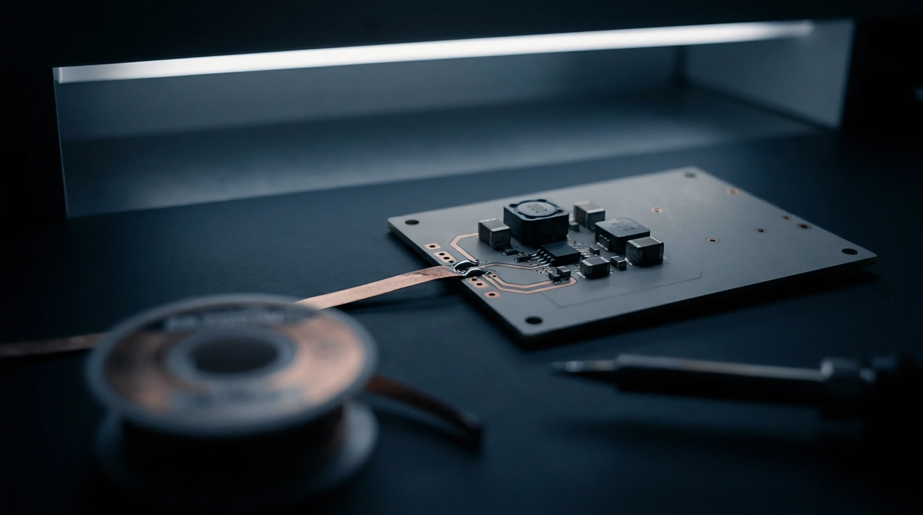
Verification of these board-level modifications demands immediate resweeps across identical frequencies to prove absolute suppression below target limits. The process repeats across distinct operating modes, verifying that high-speed memory transactions and switching power converters stay quiet under full processing loads.
Process Limitation
Field reflections and environmental RF noise invalidate open-field measurements, making fully shielded or semi-anechoic spaces mandatory for regulatory certification. When modified layouts introduce subtle parasitic coupling paths that only trigger during variable firmware execution states, static sweep routines fail to detect transient harmonic breaches. Laboratory booking schedules and high hourly facility rates also restrict repetitive iteration cycles during prototype troubleshooting.
Complete enclosure testing stops short of revealing individual trace coupling mechanisms, forcing external near-field sniffing probes onto the bare circuit board to isolate discrete radiated emission sources prior to the final chamber evaluation.