Boundary Separation
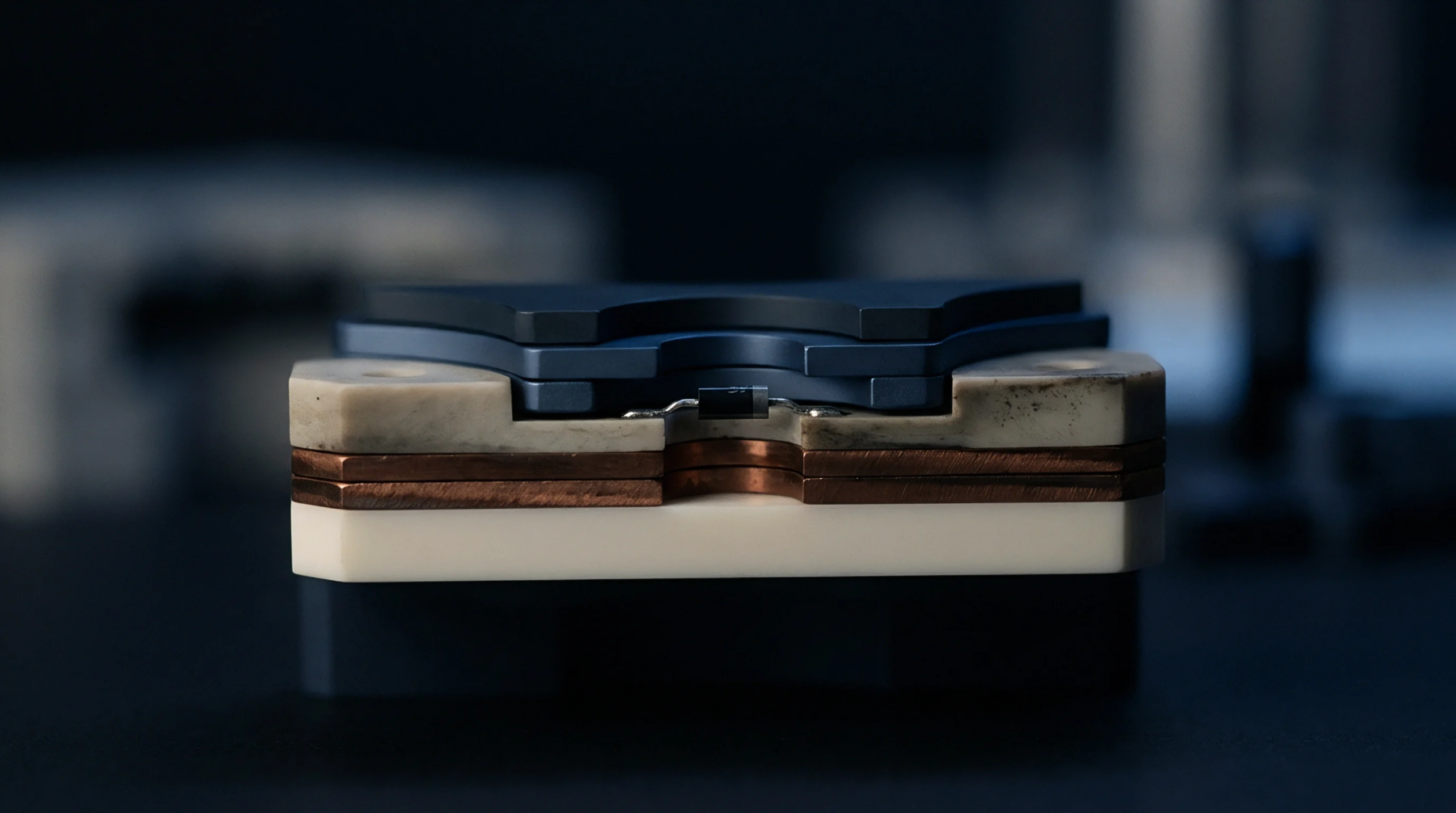
Mechanical detachment at the boundary between two dissimilar bonded materials represents a severe structural failure in microelectronic packages. This separation, identified as interface delamination, typically occurs between the silicon die and the plastic molding compound or at the lead frame interface. Moisture absorption during storage often accelerates this failure when the package undergoes high-temperature solder reflow.
The resulting internal void creates an air gap that disrupts both thermal dissipation and electrical connectivity.
Thermal Stress
Differences in the coefficient of thermal expansion among the various materials in a semiconductor package generate intense localized stresses during thermal cycling. These stresses tend to concentrate at the corners of the die, where the mismatched expansion rates of the silicon and the surrounding epoxy are most pronounced. Over repeated temperature swings, the bond between these layers degrades until interface delamination initiates and propagates across the surface.
This mechanical separation can sever the delicate gold or copper wire bonds attached to the die pads, resulting in intermittent or permanent open circuits. The damage is irreversible and frequently leads to the complete functional failure of the electronic device.
Failure Inspection
Acoustic imaging techniques easily detect these internal gaps because the air-filled void reflects nearly all the incident ultrasonic energy. High-frequency acoustic waves encounter a massive impedance mismatch at the boundary of the air gap, creating a highly visible, phase-inverted signal in the scan. Regular inspection during environmental testing helps locate these separations before they cause catastrophic failures in the field.