Operational Output
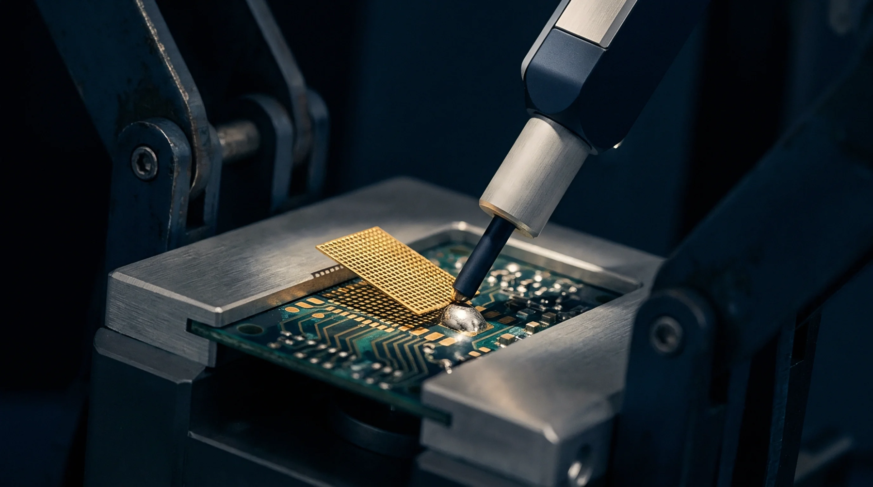
Calculating manufacturing yield requires dividing total accepted assemblies by the absolute count of units entering a specific production run on a surface mount technology line. Component placement machines and solder paste printers generate defects during active board fabrication, which demands rigorous electrical testing or optical inspection to isolate failures before final boxing. Technicians track this fraction across every shift to catch solder bridging or missing passives immediately after reflow ovens complete thermal profiling.
Strict acceptance criteria separate true assembly failures from board supplier anomalies, preventing faulty substrate laminates from skewing the statistical baseline of the manufacturing floor.
Financial Variance
Defective circuit boards demand manual rework or scrap disposition, creating direct cost variances against the initial Bill of Materials budget for that product. Labor hours spent troubleshooting solder joints on the bench consume capacity that should feed higher volume lines, reducing overall factory throughput without generating additional revenue. Scrap material accumulates quickly when paste deposition drifts out of statistical control, forcing procurement teams to expedite replacement passives at premium spot market pricing.
Engineering changes introduced halfway through a production batch invalidate existing stock, turning perfectly functional assemblies into obsolete inventory that requires immediate financial write-offs.
Process Capability
Statistical process control charts track historical yield trends to predict when stencil apertures wear out or placement heads lose calibration accuracy. Engineers establish lower control limits for each assembly stage, triggering automatic line stoppages if board failure rates exceed predefined threshold percentages during continuous running. Thermal excursions inside convection ovens alter solder wetting behavior, requiring constant profile adjustments to maintain high first-pass acceptance rates across complex double-sided printed circuit boards.
Automated optical inspection algorithms evaluate solder fillet geometry against strict IPC standards, ensuring that structural joint integrity matches the mechanical demands of the final application environment.