Thickness Variation
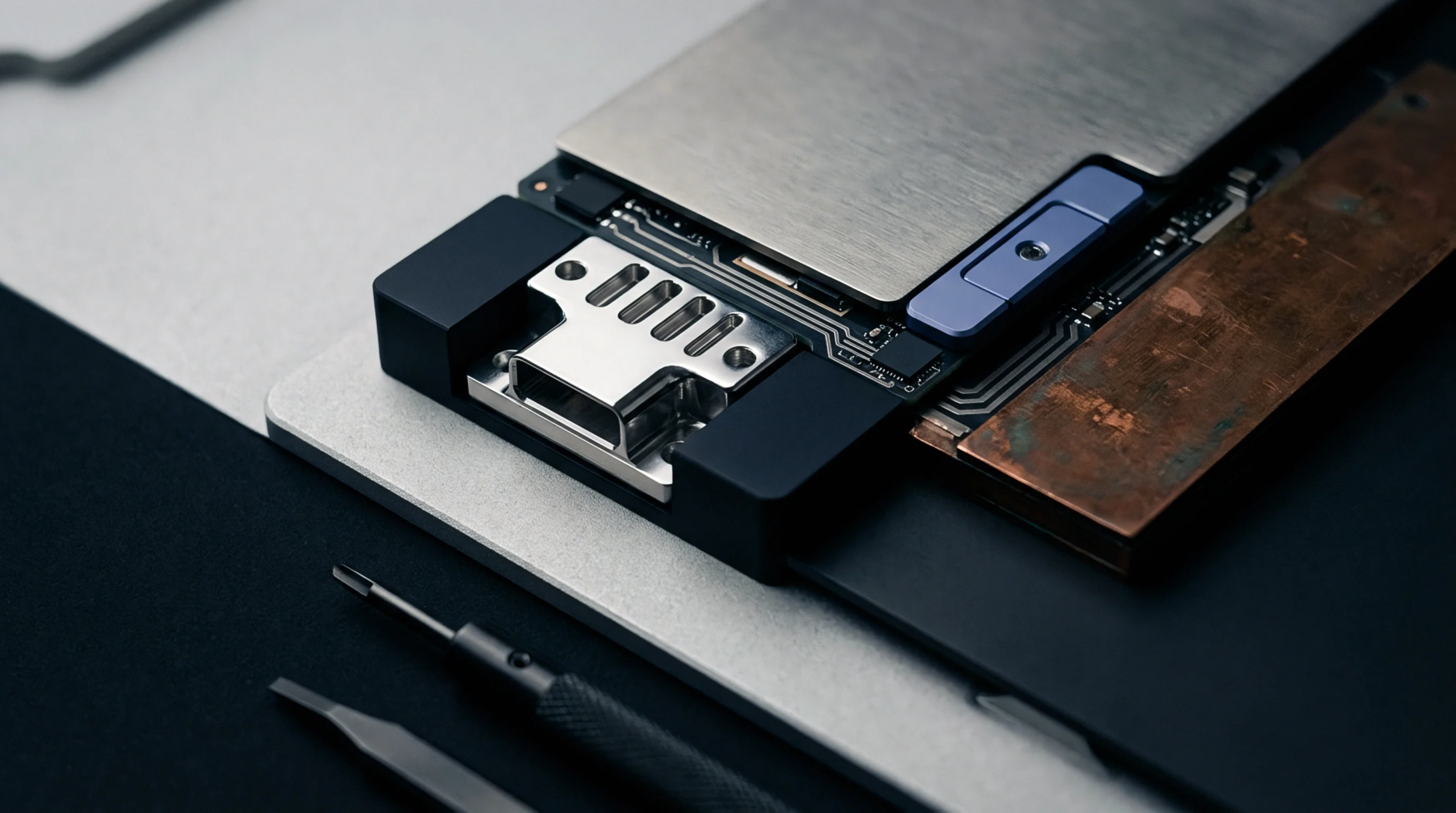
Printing plates featuring multiple foil thicknesses across their surface accommodate the differing solder volume requirements of diverse surface-mount components. The use of stepped stencils allows manufacturers to deposit thicker solder paste layers for large connectors and thinner layers for fine-pitch microcircuits on the same board. This hardware design addresses the challenge of mixed-technology component placement during assembly.
Deposition Balancing
Manufacturing of these multi-thickness foils involves chemically etching or milling localized pockets into the metal sheet. When stepped stencils are deployed on the assembly line, the squeegee blade must adapt to the physical height transitions to ensure uniform paste application. This technique avoids the problem of excess solder causing short circuits on small components while preventing starvation on larger terminals.
Printing Optimization
Process engineers must carefully calculate the size and depth of the stepped regions to prevent premature squeegee wear and paste scooping. Incorrect step design can lead to inconsistent paste release and poor deposit definition near the transition zones. Therefore, the distance between the stepped pockets and adjacent fine-pitch components must meet strict design-for-manufacturability guidelines.
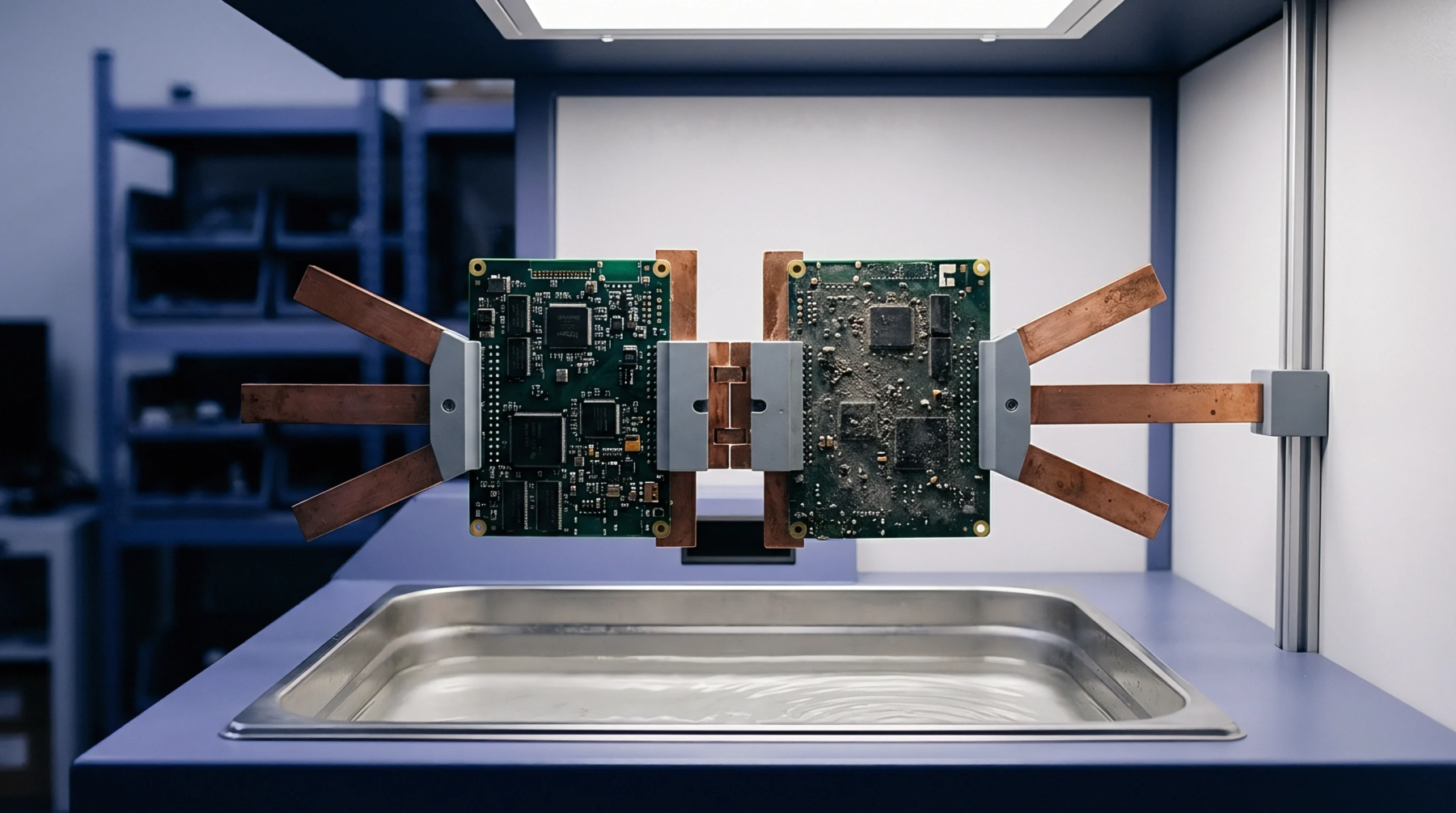
Properly implemented foils improve soldering yields across boards that combine heavy power components with high-density micro-BGAs, ensuring that every pad receives the correct volume of paste without requiring separate printing passes. This localized adjustment of thickness represents a highly effective method for managing solder volume distribution on complex electronic assemblies.