Metrological Technique
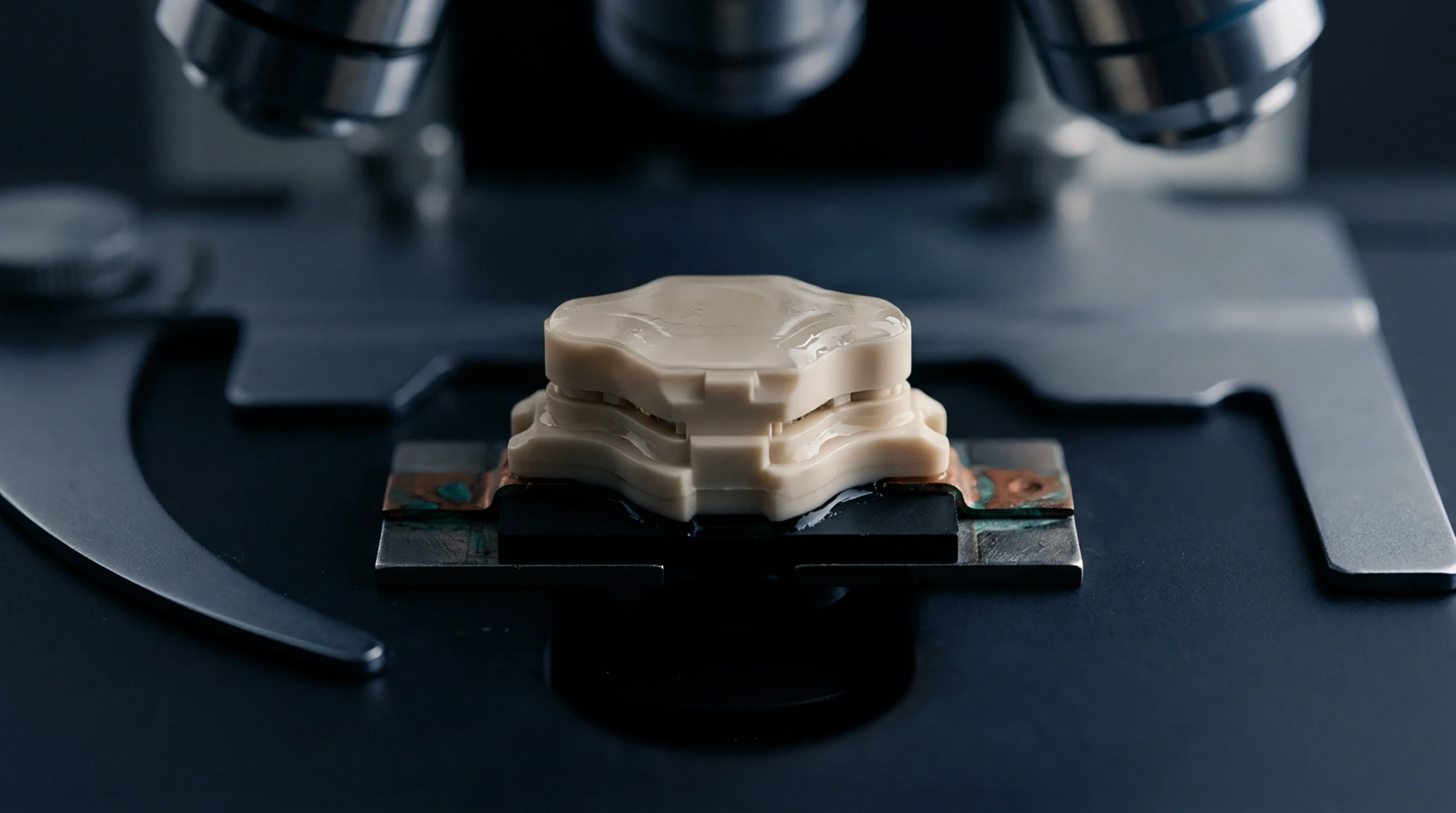
Optical and sensor-based metrology methods trace dimensional shifts across structural components and substrate panels during controlled heating and cooling cycles. Through thermal displacement mapping, test engineers visualize localized expansion and mechanical distortion across press platens and multilayer circuit boards under actual operating temperatures. Data collection combines laser triangulation sensors or non-contact capacitive probes arranged in a high-density grid.
As temperatures rise from room ambient to curing levels, software captures three-dimensional positional changes at hundreds of surface points. The resulting dataset produces contour maps showing magnitude and direction of vector displacements across the surface. Analysis reveals non-linear thermal expansion caused by material anisotropy, uneven heating element distribution, or internal structural constraints.
Diagnostic Application
Equipment manufacturers use surface deformation tracking to evaluate press frame rigidity and platen heater design. Inputting thermal displacement mapping data into finite element models validates thermal stress calculations and identifies mechanical binding risks in platen guide pins. In PCB panel fabrication, this technique pinpoints areas prone to warp and twist, allowing process engineers to modify copper balance on inner layers.
Identifying localized thermal hot spots early prevents high-volume production yields from dropping due to layer misregistration.
Accuracy Threshold
Sensor calibration and environmental isolation govern the spatial resolution achievable during thermal testing. When ambient temperature fluctuations affect optical mounting frames, thermal displacement mapping introduces measurement artifacts that distort displacement vectors. Standard procedures require optical laser sensors with sub-micron resolution calibrated against low-expansion invar reference targets.