Impedance Profile
Conductive pathways that link drivers to receivers on a printed circuit board must maintain controlled physical dimensions to preserve signal integrity at high frequencies. Transmission lines behave as distributed parameter networks where inductance and capacitance govern the propagation velocity of electromagnetic waves. High speed digital assemblies require copper trace widths and dielectric thicknesses to remain uniform across the entire routing path to prevent reflections.
Discontinuities in geometry cause impedance mismatches that degrade eye diagram margins during digital data transfer.
Termination Strategy
Matching source impedance to trace impedance absorbs incident wave energy and suppresses ringing on the receiving pin. Designers place surface mount resistors at either the driver output or the receiver input depending on the topology of the net. Series dampening resistors add nominal resistance to slow edge rates while parallel configurations pull the voltage level to a defined rail.
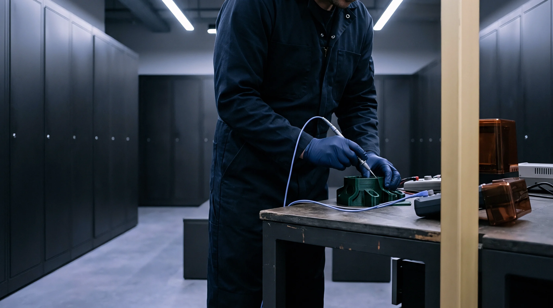
Oscilloscopes capture voltage reflections during time domain reflectometry testing to verify that terminations eliminate standing waves.
Crosstalk Control
Parallel traces running in close proximity experience capacitive and inductive coupling that injects noise into quiet victim nets. Manufacturing standards specify minimum edge to edge spacing rules relative to the distance between the conductor and the reference plane. Ground shields or guard traces inserted between differential pairs absorb stray electric fields and reduce mutual inductance across the laminate layer stackup.
Automated optical inspection equipment verifies trace separation dimensions on inner layers before lamination seals the internal circuitry.