Fixturing Mechanics Strain Limits and Test Point Access Placement Rules
Fixture mechanics prevent board damage by holding strain below five hundred microstrain and enforcing forty-mil minimum test point pad spacing.


Deflection
A bed of two thousand test pins exerts over four hundred Newtons of upward thrust against an unbacked FR4 panel during in-circuit testing. When an automated mechanical or vacuum fixture pulls the circuit board down onto the target lands, uneven pin resistance bows the panel locally. That mechanical distortion concentrates bending moments directly beneath surface-mount solder joints.
Multilayer ceramic capacitors and ball grid array packages lack the compliance to absorb shear, leaving copper pads vulnerable to tearing out of the resin matrix. The test console may register an electrical pass even after the internal ceramic dielectric has cracked or a corner solder ball has separated from its trace.

Mechanical Load Accumulation across Bed Assemblies
Individual pogo contacts exert between two and ten ounces of compressive resistance at nominal travel. Dense power rails, ground planes, and wide memory interfaces require tightly grouped probes to measure continuity and resistance accurately. A cluster of fifty pins on fifty-mil pitch concentrates twenty-five pounds of vertical reaction force within an area smaller than a postage stamp.
Without backstops directly behind the cluster on the reverse side of the board, the substrate flexes downward around the perimeter while bowing upward at the pin field.
Peak mechanical resistance across a two-thousand-pin bed-of-nails fixture reaches four hundred Newtons under standard eight-ounce spring assemblies during full engagement.
Substrate thickness dictates flexural rigidity: standard one-point-six millimetre laminate deflects four times farther than an otherwise identical two-point-four millimetre board under the same contact forces. Thinner panels measuring zero-point-eight millimetres exhibit localized oil-canning, snapping between convex and concave profiles as probe spring limits engage. This dynamic snap-through generates violent acceleration transients across neighboring components.
Unconstrained board bending during fixture actuation generates distinct electrical and physical failure modes across assembled components:
- Pad cratering shears the resin matrix beneath surface trace copper, detaching fine-pitch solder balls without immediate electrical disconnect.
- Capacitor cracking propagates through internal barium titanate dielectric layers, causing delayed low-resistance leakage paths or catastrophic thermal runaway during powered field operation.
- Solder joint fracturing cleaves intermetallic compound layers at the component interface, leaving microscopic air gaps that open under subsequent thermal expansion.
- Internal via tearing breaks barrel plating inside inner signal layers, producing intermittent opens that evade static bed-of-nails screening.
Solder joint failure curves depend directly on engagement velocity. Rapid pneumatic clamping drives strain rates beyond acceptable limits, turning what would be manageable elastic bending under slow displacement into brittle fracture. Mechanical designers must therefore constrain overall laminate displacement within tight geometric windows to safeguard component reliability.

Substrate Warpage during Vacuum Holddown
Differential air pressure pulls the bare laminate downward against the seal perimeter while spring contacts resist the movement. Standard atmospheric draw creates up to fourteen pounds per square inch of distributed clamping force. An uneven distribution of test pins across the panel produces severe pressure differentials, pulling unprobed zones downward into the vacuum chamber while probed areas stay elevated.
Over time, perimeter gasket wear often imparts a permanent dish distortion across rectangular boards when peripheral probe density fails to balance atmospheric loads.
Uncontrolled board bending during production testing causes intermittent field opens that multiply warranty reserves and force premature batch recalls.


Platen
Upper press frames transmit clamping force directly through push fingers down to the bare laminate while the carrier plate absorbs travel. Proper alignment between the moving upper pusher array and the stationary lower probe field governs whether vertical forces neutralize one another or generate destructive shear moments. Machining errors in the backing plate or inaccurate clearance cuts around tall surface-mount devices introduce uneven point loads that crack component packages.

Pneumatic versus Mechanical Actuation Dynamics
Air cylinders drive the moving assembly with rapid acceleration curves that peak upon initial contact. In pneumatic test fixtures, an uncontrolled exhaust stroke slams the top platen onto the board assembly, transferring severe kinetic shock into the laminate before spring probes compress smoothly. Electromechanical screw-driven fixtures regulate closure speed throughout the stroke, maintaining linear travel velocities below twenty millimetres per second.
Controlled descent velocity reduces the peak microstrain rate by half compared to unregulated pneumatic drops.
| Actuation Mechanism | Closure Velocity (mm/s) | Peak Contact Force (N) | Maximum Strain Rate (µε/s) | Primary Mechanical Risk |
|---|---|---|---|---|
| Unregulated Pneumatic | 80 to 150 | 650 to 900 | 12000 to 25000 | Kinetic shock impact cracking |
| Regulated Pneumatic with Dampers | 25 to 50 | 450 to 600 | 4000 to 8000 | Localized seal edge bending |
| Electromechanical Servo Press | 5 to 15 | 400 to 550 | 800 to 2500 | Over-compression at hard stops |
| Manual Clamshell Lever | Variable manual | 300 to 700 | 2000 to 15000 | Operator-induced asymmetric torsion |

Has Fixture Pushout Exceeded Plate Tolerances?
Pressure fingers machined from G10 or ESD-safe polyetheretherketone bend slightly under prolonged cyclic service. Continuous contact fatigue distorts push rods, shifting their contact footprints away from designated bare laminate zones and onto fragile passives. Fixture design rules require push fingers to align directly over opposite-side bottom support pins within a circular tolerance window of zero-point-five millimetres.
Misalignment creates an offset couple, generating pure torsional bending across the intervening FR4 dielectric.

Support Pin Distribution Patterns
Anvils positioned beneath dense probe clusters absorb vertical thrust before the laminate bows. Machinists place stationary tooling pins through open drill holes or directly beneath wide unpopulated ground areas on the bottom layer. The clearance distance between any support anvil edge and adjacent surface-mount solder joints cannot drop below one millimetre.
When clearance tolerances vanish, the rigid anvil pin strikes adjacent solder fillets during fixture engagement, fracturing the joint through direct mechanical interference.
Standard thirty-day shop allowances often tolerate minor top-plate bowing, but contact alignment requires rigid, unyielding platens to prevent component strikes.


Threshold
Circuit laminates experience severe localized tensile forces around solder joints whenever unbacked test pins depress the raw FR4 surface. Mechanical strain quantifies the fractional deformation of the board material under load, expressed in microstrain where one unit equals one micrometre of displacement per metre of length. High-reliability manufacturing programs define explicit strain limits to prevent pad cratering, component cracking, and trace fracturing during every fixtured assembly operation.

Strain Rate Dependency under Standard Regimes
Brittle failure modes multiply as the speed of mechanical deformation accelerates during bed closure. Materials withstand higher absolute strain when the load applies slowly, allowing polymer chains in the epoxy laminate to undergo viscoelastic relaxation. Rapid impact loading eliminates this compliance, forcing the copper-resin interface into catastrophic brittle rupture.
IPC-JEDEC-9704A defines an inverse relationship between allowable peak microstrain and the measured strain rate.
IPC-JEDEC-9704A annex tables disqualify lot shipments whenever principal diagonal strain exceeds five hundred microstrain at actuation velocities above one hundred millimetres per second.
Strain measurement protocols require triaxial rosette gauges soldered directly adjacent to sensitive components during fixture qualification. The setup procedure follows a strict technical sequence:
- Surface preparation removes all solder mask residue, contaminants, and flux residues from the target board zone down to bare resin or solid plane.
- Adhesive dispensing applies cyanoacrylate bonding agent across the gauge backplate with uniform thickness below twenty micrometres.
- Rosette positioning locates the measuring grids within one millimetre of the targeted component corner, oriented parallel to package edges.
- Thermal stabilization holds the assembly at ambient laboratory conditions for twelve hours to eliminate residual chemical curing stress.
The rosette outputs three strain channels, designated as epsilon a, epsilon b, and epsilon c. Calculating the principal strains requires resolving these channel outputs into orthogonal components using standard Mohr circle equations. The maximum principal strain and minimum principal strain indicate the true state of multi-axis board deformation.

Rosette Placement near Brittle Ceramic Components
Triaxial foil sensors bonded within one millimetre of solder fillets capture orthogonal and shear vectors simultaneously. The primary risk zone sits at the four corners of rigid ball grid array devices, where thermal mismatch and mechanical lever arms concentrate peak loads. Placing rosettes further than one-point-five millimetres from the package boundary understates actual package corner strain by as much as forty percent.
Finite element analyses confirm that strain decay gradients around stiff packages drop steeply across small radial distances.
| Board Thickness (mm) | Strain Rate: 100 µε/s | Strain Rate: 1000 µε/s | Strain Rate: 10000 µε/s | Maximum Hard Ceiling (µε) |
|---|---|---|---|---|
| 0.8 | 575 | 425 | 310 | 600 |
| 1.0 | 690 | 510 | 370 | 720 |
| 1.6 | 1035 | 765 | 560 | 1080 |
| 2.0 | 1265 | 935 | 685 | 1320 |
| 2.4 | 1500 | 1105 | 810 | 1560 |
| Values reflect allowable diagonal principal strain for standard FR4 laminate assemblies with SAC305 solder attachments under IPC-JEDEC-9704A guidelines. | ||||

Worked Calculation for Allowable Microstrain Limits
Assume an eight-layer board measuring one point six millimetres thick with ball pitch set at zero point eight millimetres. During pneumatic bed-of-nails fixture closure, high-speed data acquisition samples the three gauge channels at ten kilohertz. The channel readings register at a single time step: epsilon a equals three hundred and twenty microstrain, epsilon b equals one hundred and eighty microstrain, and epsilon c equals negative forty microstrain.
The angle between channels measures forty-five degrees.
The maximum principal strain calculation uses the standard formulation:
Epsilon maximum equals half of the sum of epsilon a and epsilon c, plus the square root of half the square of the difference between epsilon a and epsilon c, added to the square of epsilon b minus half the sum of epsilon a and epsilon c.
Summing channels a and c gives two hundred and eighty microstrain. Half of this sum yields one hundred and forty microstrain. The difference between channels a and c equals three hundred and sixty microstrain, half of which is one hundred and eighty.
Squaring one hundred and eighty yields thirty-two thousand four hundred. Epsilon b minus one hundred and forty leaves forty microstrain, whose square equals one thousand six hundred. Adding these squares produces thirty-four thousand.
Taking the square root of thirty-four thousand gives one hundred and eighty-four point four microstrain.
Adding one hundred and forty to one hundred and eighty-four point four results in a maximum principal strain of three hundred and twenty-four point four microstrain. If the measured strain rate reaches seven thousand microstrain per second, the allowable limit for a one-point-six millimetre laminate under IPC-JEDEC-9704A interpolates to six hundred and ten microstrain. The calculated three hundred and twenty-four point four microstrain sits safely below the upper boundary.
The fixture actuation earns engineering sign-off for that specific component location.
IPC-JEDEC-9704A paragraph 5.2 defines the acceptable microstrain boundary against step-rate velocity, removing ambiguity from supplier dispute meetings.


Pitch
Automated bed testers require distinct land targets positioned across bottom and top copper layers. Layout designers balance spatial density against electrical verification access, fitting target pads between routed traces, vias, and passive packages. When test points crowd adjacent component lands, mechanical tolerances stack up, causing wandering probe heads to glance off pad edges and strike delicate component bodies.

Annular Ring Geometry and Probe Centering
Drill registration tolerances accumulate across manufacturing stages, shifting the copper barrel relative to the target center. A dedicated test land requires a bare metal target diameter matched to the probe style. Fifty-mil spring probes demand target diameters between zero-point-seven and zero-point-nine millimetres to ensure consistent hit rates across thousands of cycles.
Smaller thirty-nine-mil probes can strike zero-point-six millimetre lands, but probe tip wandering increases contact resistance and triggers false open readings.
Solder mask encroachment over probe targets drives false open readings during automated bed tests.
Solder mask clearances must clear the copper target diameter by zero-point-one millimetres around the entire perimeter. Solder mask encroachment onto the pad shoulder lifts the probe chisel tip, breaking the electrical connection or deflecting the shaft sideways. The lateral deflection side-loads the internal spring, accelerating probe barrel wear and generating particulate debris inside the fixture bed.

Are Staggered Patterns Effective below Fifty Mils?
Linear rows of spring pins placed on thirty-mil centers create extreme local pressure lines across fragile laminate weaves. Staggering test points in triangular or zig-zag patterns disperses contact forces across a wider surface area. Shifting alternate targets by zero-point-five millimetres laterally doubles the effective distance between adjacent drill holes in the probe plate.
This spacing preserves the structural web thickness of the fixture platen and eliminates cross-drilling breakthrough during socket installation.
| Probe Center Pitch | Minimum Target Diameter (mm) | Target-To-Target Center (mm) | Pad-To-SMD Edge Clearance (mm) | Probe Retention Method |
|---|---|---|---|---|
| 100 mil (2.54 mm) | 1.00 | 2.54 | 1.25 | Standard Press Receptacle |
| 75 mil (1.91 mm) | 0.85 | 1.91 | 1.00 | Standard Press Receptacle |
| 50 mil (1.27 mm) | 0.70 | 1.27 | 0.75 | Miniature Press Receptacle |
| 39 mil (1.00 mm) | 0.55 | 1.00 | 0.50 | Direct Socketless Sleeve |
Package Keep-Out and Component Clearances
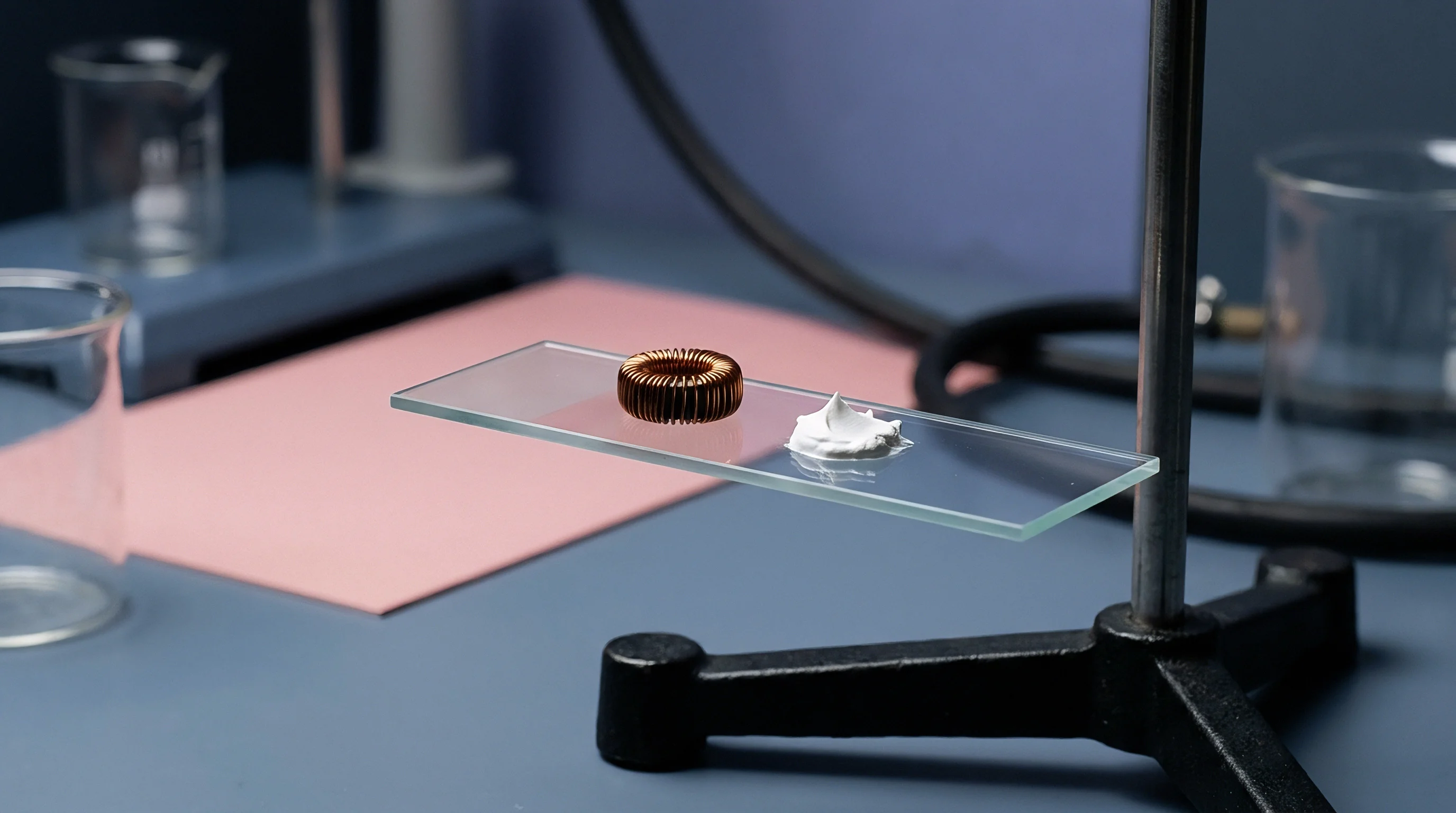
Tall electrolytic capacitors and molded inductors obstruct top-side fixture hardware during engagement strokes, where tight clearances risk direct collisions. The mechanical boundary around tall devices must accommodate fixture push rods, vacuum sealing gaskets, and lateral plate tolerances.
Critical spacing rules dictate clearance zones around surface-mount devices and board features:
- Tall component boundaries demand a minimum horizontal clearance of two-point-five millimetres from the component body to the center of any test target.
- Tooling pin perimeters require five millimetres of clear annular space to seat fixture alignment bushings without fouling surface traces.
- Board edge margins require three millimetres of untouched clearance along clamped edges to prevent interference with conveyor rails and vacuum seals.
- Through-hole lead ends demand one-point-five millimetres of separation from test points to prevent bent leads from shorting against spring barrels.
Fixture maintenance programs recalibrate probe alignment after every fifty thousand actuations to clear accumulated flux, correct drift, and preserve targeting precision. Neglecting these rules degrades first-pass test yields and exposes bare circuit boards to localized punch shear failures.
Generous spacing around tall components prevents probe barrel interference and protects brittle glass envelopes.


Release
Production authorization requires documented strain gauge logs signed by both manufacturing and quality leads. An uncertified test fixture represents an uncontrolled mechanical press capable of destroying thousands of assemblies before defect patterns emerge in field return data. Importers and tier-one buyers demand primary test proof, including raw microstrain waveforms and calculated principal strain curves, before authorizing high-volume board production.
Support pins placed directly opposing dense test clusters prevent board flexure during rapid mechanical engagement.

Strain Gauge Certification Sign-Off Protocol
The qualification file pairs raw voltage waveforms against time-domain strain plots for every primary sensor location. A compliant certification package contains specific physical records. Technicians verify sensor calibration, bridge excitation voltages, and shunt calibration factors before mounting gauges to pristine first-article boards.
The test protocol runs the board through five consecutive fixture cycles, recording peak microstrain, step-rate velocity, and residual offset strain after platen release.
Residual offset strain indicates non-elastic damage. When a board fails to return to its baseline flat state after fixture disengagement, the FR4 matrix has suffered permanent plastic deformation or internal copper delamination. Any residual offset exceeding fifty microstrain mandates immediate fixture rejection and physical anvil re-engineering.

Batch Conformance and Landed Exposure
Shipments reaching overseas ports face immediate commercial quarantine if unmonitored test fixtures crack component terminations. When customs inspectors or customer quality auditors discover cracked multi-layer ceramic capacitors, the buyer faces total batch recall expenses, air freight replacements, and immediate factory line stoppages. Contractual test clauses allocate liability directly to the manufacturing partner unless the factory presents validated, dated strain qualification dossiers matching the exact tool serial number used during production.
Whether cumulative microstrain damage from repeated test actuations accelerates long-term solder fatigue in harsh automotive environments remains an open engineering question.