Structural Reinforcement
Methods used to stop the separation of copper pads from the resin and glass layers of a printed circuit board focus on reducing mechanical stress at the interface. Successful pad cratering prevention often starts with the selection of high Tg laminates that offer better adhesion and lower thermal expansion. Design choices such as increasing the pad size or using non solder mask defined pads can also distribute the load more evenly across the dielectric surface.
This prevents the formation of craters that lead to open circuits or intermittent failures in the field.
Mechanical Mitigation
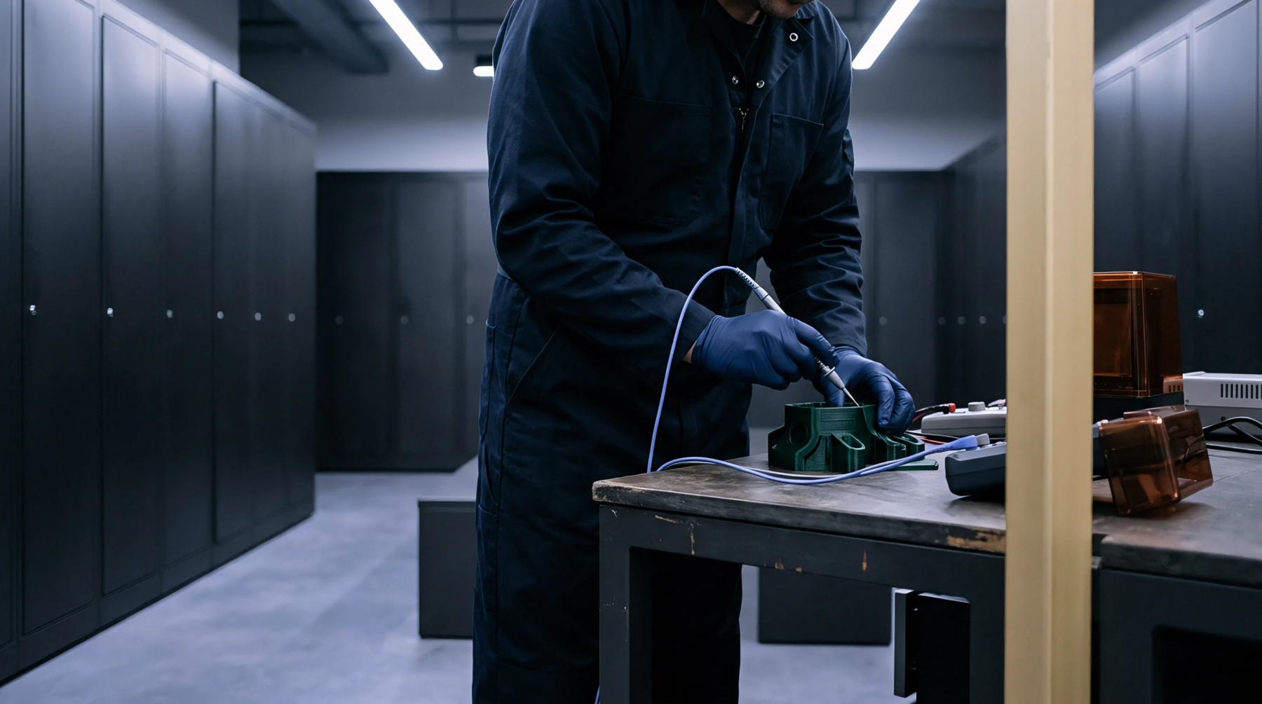
The handling of the board during assembly and testing represents the period of highest risk for this type of failure. Standard pad cratering prevention protocols require the use of support pins during in-circuit testing to prevent the board from bending.
Process Control
Reflow temperatures and cooling rates are monitored to minimize the residual stresses that develop between the copper and the laminate. If the assembly undergoes multiple heat cycles, the risk of the pad lifting increases, making pad cratering prevention a factor in the rework strategy. The final inspection looks for subtle micro cracks in the resin beneath the pad which indicate that the adhesive strength has been compromised.