Layer Accumulation
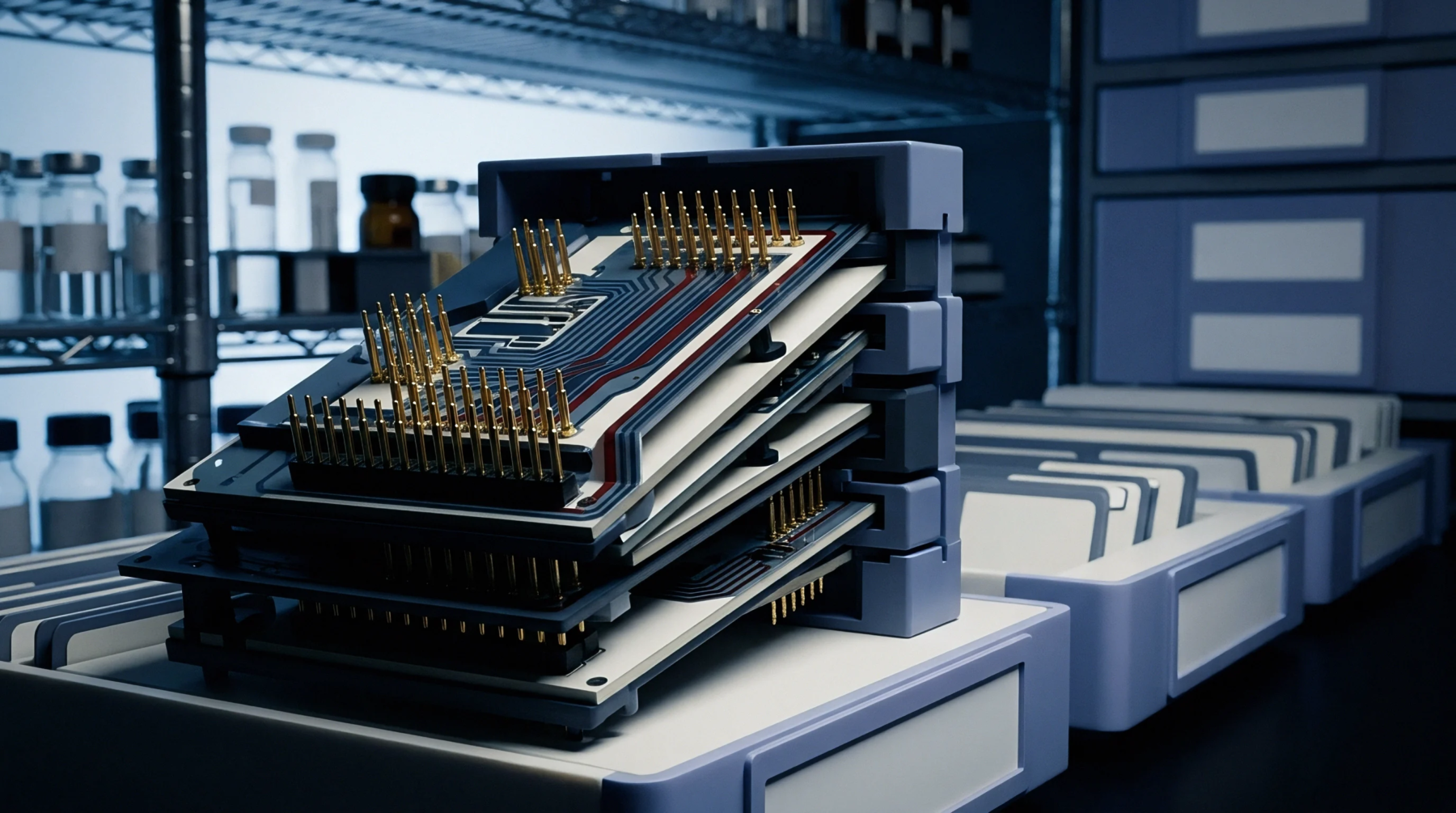
The step-by-step addition of unreinforced dielectric layers and microvia interconnects onto an etched structural base core enables the manufacture of high-density interconnect printed circuit boards. Through repeated cycles of lamination, laser via drilling, chemical desmear, metallization, and lithographic copper patterning, sequential buildup constructs high-density routing layers that support fine-pitch area-array components. This additive methodology supersedes conventional through-hole multilayers by utilizing blind and buried microvias, stacked or staggered across buildup tiers, to escape thousands of input-output pins on millimeter-scale semiconductor packages.
Structural verification requires microsectioning each buildup cycle to inspect microvia barrel integrity, target pad capture margins, and dielectric thickness per IPC-6012 specifications.
Fabrication Cycle
Process workflows begin with a fully cured, double-sided or multi-layer core that has been laminated, drilled, plated, and photolithographically etched. An unreinforced dielectric film, such as resin-coated copper or silica-filled epoxy, is vacuum-laminated over the prepared core surfaces, after which ultraviolet or carbon dioxide lasers ablate microvias down to internal landing pads. Desmear chemistries clean residual dielectric debris from the hole bottoms before electroless copper deposition coats the hole walls, followed by electrolytic copper plating to fill or line the microvia cavities.
Photolithography patterns the outer copper layer, after which the entire sequence repeats for subsequent layer additions until reaching the target layer count.
Thermal Reliability
Multiple lamination and thermal cycles expose the accumulated dielectric and metallization layers to cumulative thermo-mechanical strain. Mismatches in the coefficient of thermal expansion between dielectric layers and electrolytic copper microvias can provoke interfacial separation, corner cracking, or target pad pull-away during subsequent surface mount assembly reflow. Fabricators audit buildup integrity by subjecting testing coupons to repeated thermal shock and thermal cycling tests per IPC-TM-650, monitoring resistance shifts via four-wire Kelvin probes.
Sequential buildup provides the interconnect density necessary to route advanced ball grid array devices on modern computing platforms.