Capacitance Architecture
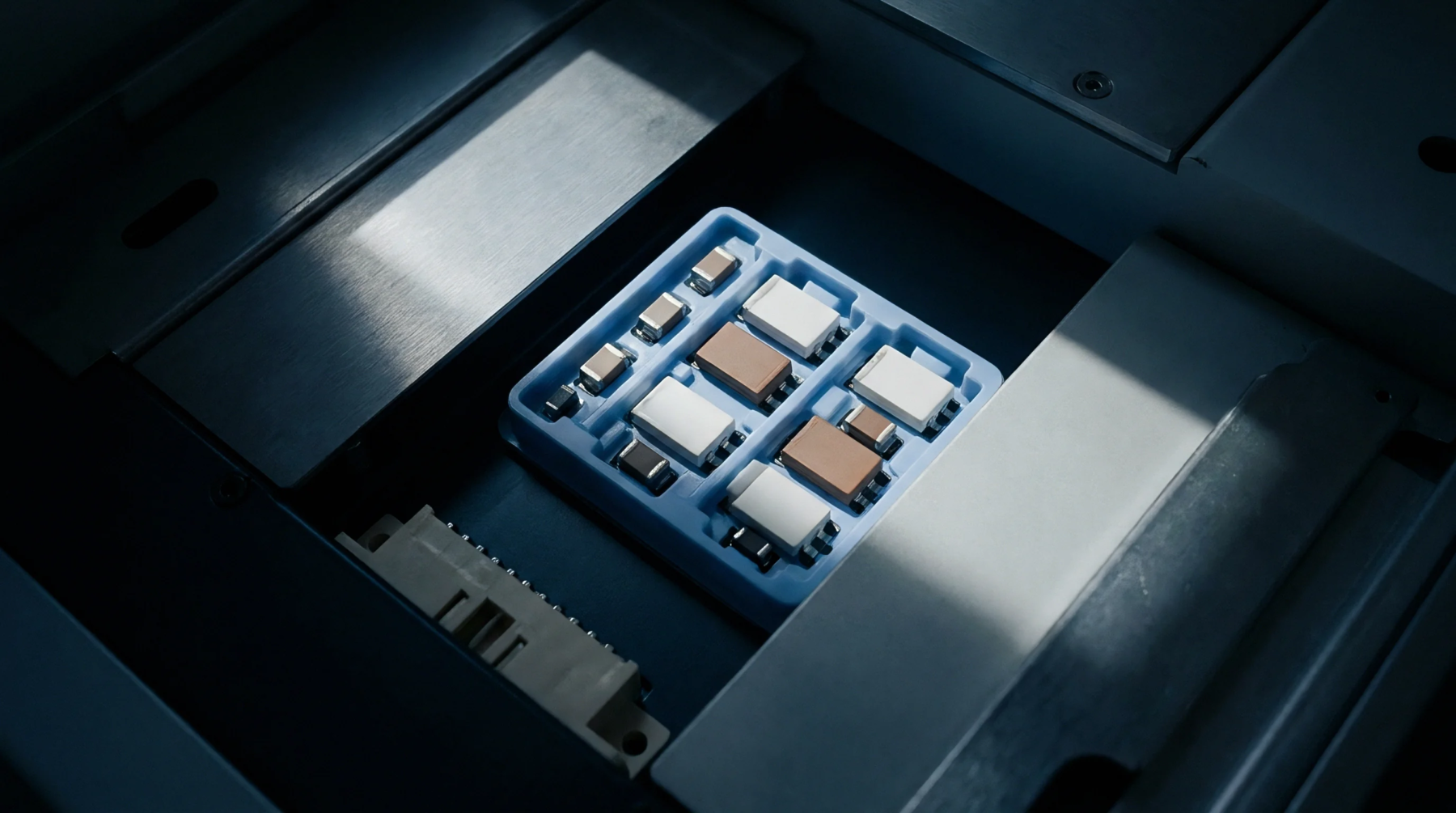
Decoupling networks require careful distribution of passive components across multi-layer printed circuit boards to maintain signal integrity. A stitching capacitor bridges separated ground planes or power domains near high-speed signal transitions to provide a low-impedance return path for electromagnetic interference mitigation. High-frequency transient currents find a localized escape route through this placement, preventing unwanted noise radiation across peripheral circuits.
Modern automated optical inspection systems verify solder fillet formation at both component terminations during surface mount technology processing. Thermal cycling loads during wave soldering or vapor phase reflow testing challenge the mechanical reliability of these solder joints.
Resonance Suppression
High-speed digital logic produces harmonics that excite cavity resonances within internal power and ground planes. A stitching capacitor dampens these parallel-plate oscillations by introducing targeted losses and shifting the resonant frequency outside the operational spectrum of the device. Differential signaling pairs benefit directly from this stabilization because voltage fluctuations on the reference planes degrade jitter margins.
Component engineers calculate the required capacitance value based on dielectric thickness and plane spacing parameters defined in the layout specifications. Manufacturing defects such as micro-cracking in the ceramic dielectric material manifest during in-circuit testing as sudden dielectric breakdown or excessive leakage current.
Placement Constraints
Strict geometric rules govern the physical location of decoupling elements relative to high-density ball grid array packages and via transitions. A stitching capacitor must sit as close as possible to the target reference plane discontinuity to minimize inductive parasitics introduced by trace routing lengths. Production lines utilize high-speed pick and place machinery equipped with force-feedback sensors to prevent mechanical fracture of fragile ceramic bodies during placement.
Automated X-ray inspection evaluates internal voiding percentages beneath bottom-terminated packages to guarantee thermal and electrical performance over time. Quality control engineers analyze test data from bed-of-nails fixtures to detect marginal soldering defects before assemblies enter final enclosure integration.