
Identifying Printed Circuit Board Defect Limits in High Speed Differential Lines
High-speed differential lines require guard-banded TDR and VNA coupon testing to prevent localized trace defects from causing field failure escapes.
High-speed differential lines require guard-banded TDR and VNA coupon testing to prevent localized trace defects from causing field failure escapes.
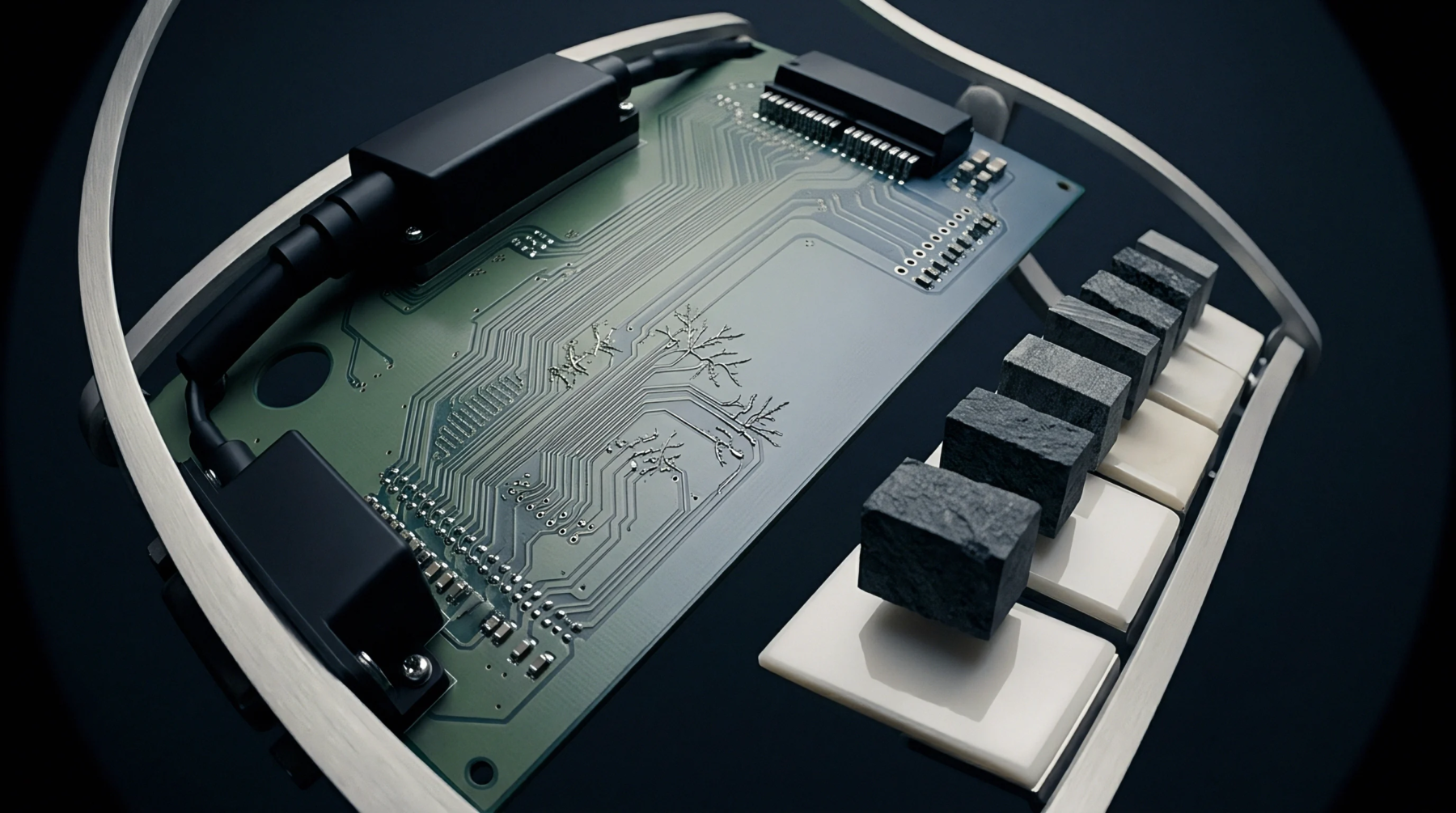
Etched sidewall taper concentrates high-frequency current into edge micro-roughness, doubling conductor losses above 50 GHz unless controlled by mSAP.
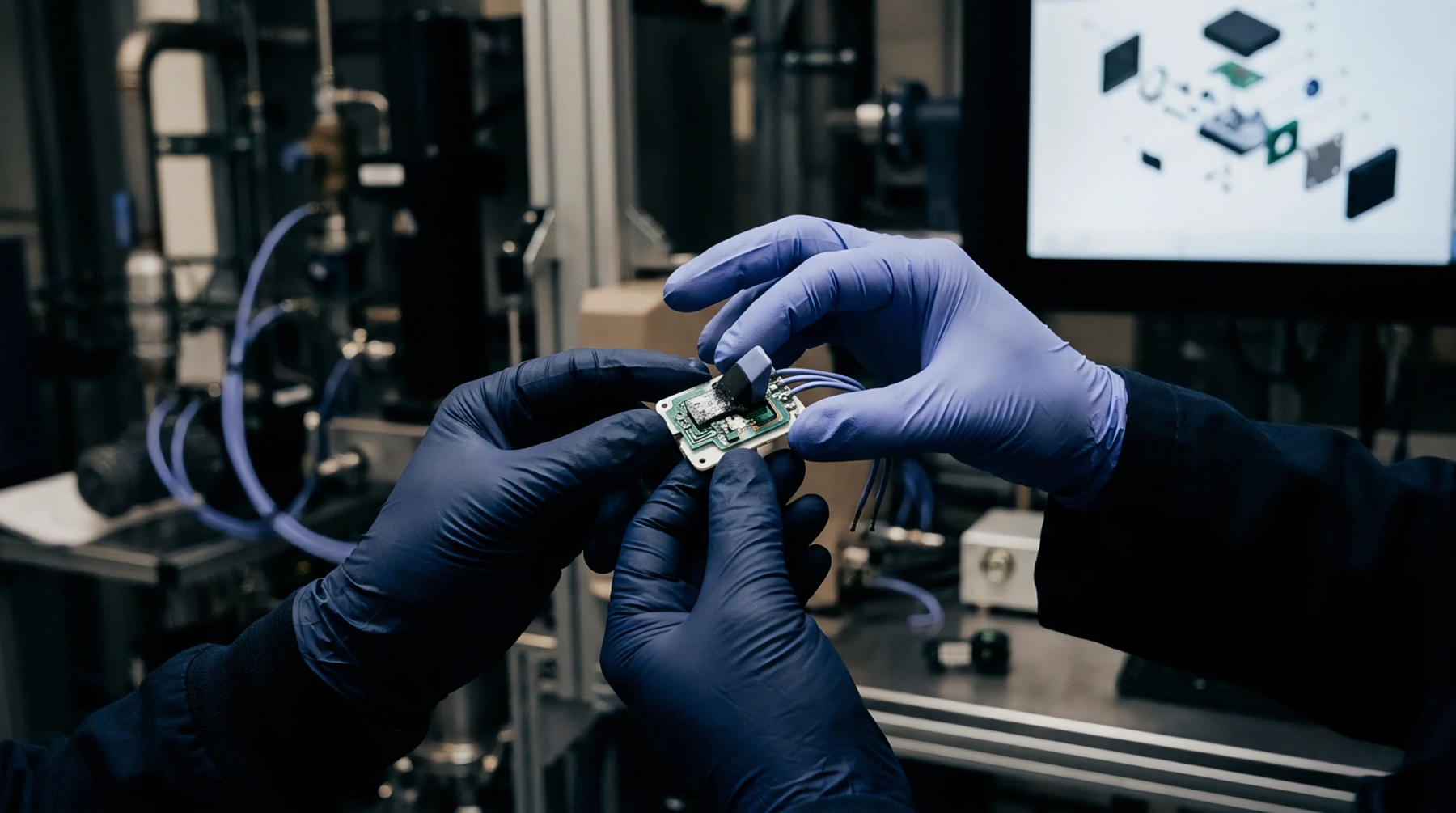
Electroless copper seed thickness variations widen flash etching dwell times, causing severe lateral undercut, collapsed etch factors, and impedance scrap.
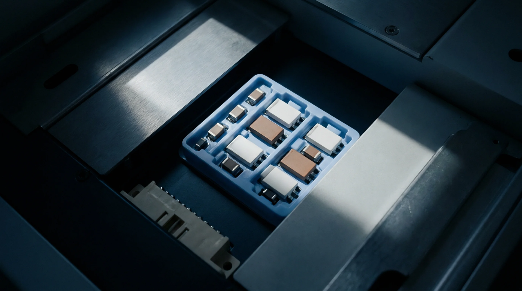
Etch fluid pooling creates trace asymmetry, changing high-frequency conductor profiles and driving insertion loss variations across printed circuit panels.

Standard IPC coupons placed along panel waste borders verify plating, registration, and impedance without consuming functional board surface area.

Semi-additive yield depends on seed layer adhesion, lithographic trench verticality, and differential etch undercut control across sequential build-up layers.

mSAP yield optimization requires balancing electroless seed thickness tolerances within ten percent to prevent flash etch trace undercut and impedance failures.
Sub-sixty micron trace fabrication mandates semi-additive processing over subtractive etching to eliminate undercut and hold tight differential impedance.
Expertise is a utility, not a secret. sentiention™ publishes its working knowledge as open reference: intelligence layer covering the materials it sources, the markets it enters, and the reference that serves both.