Microvia Interfacial Delamination Detection Using High Frequency Scanning Microscopy
High frequency scanning acoustic microscopy detects sub-micron microvia target pad delamination through radio frequency phase inversion analysis before stress fails the board.


Coupling
Ultrasonic waves traveling through liquid delivery media reflect at density boundaries inside high-density interconnect circuit structures. High-frequency scanning acoustic microscopy operates by directing focused high-frequency acoustic pulses into printed circuit board laminates and capturing the returning echoes. The physical interaction between the ultrasonic beam and internal material boundaries determines whether an interfacial gap appears as an acoustic anomaly.
When a high-frequency acoustic wave encounters an interface between two solid materials, the proportion of reflected sound pressure depends directly on the specific acoustic impedance of each material layer. Acoustic impedance equals the product of mass density and longitudinal speed of sound within that medium.

Acoustic Reflection Mechanics at Copper Interfaces
Interfacial boundaries between solid materials govern signal propagation according to local mass density and acoustic velocity differences. Electrodeposited copper target pads present a high acoustic impedance value, typically around 44.6 mega-Rayls, derived from a density of 8.96 grams per cubic centimeter and a longitudinal acoustic velocity of 4,980 meters per second. FR-4 resin matrices and glass-reinforced laminate layers present significantly lower acoustic impedance values, typically ranging from 2.8 to 3.5 mega-Rayls.
When acoustic energy travels from dielectric resin into solid copper, approximately 73 percent of the pressure amplitude reflects back toward the piezoelectric transducer. The remaining 27 percent transmits into the target pad structure.
An interfacial separation or micro-void at the base of a microvia replaces the copper-to-copper or copper-to-resin contact with a localized gas gap or vacuum void. Air presents an acoustic impedance of approximately 0.0004 mega-Rayls. The acoustic impedance mismatch between electrodeposited copper and an internal air gap approaches infinity in practical acoustic measurement terms.
A reflection coefficient exceeding 0.99 occurs at a copper-air interface regardless of acoustic frequency, producing full phase inversion on the A-scan waveform.
Air stops acoustic transmission entirely. Virtually 100 percent of the incident acoustic pressure reflects directly from the top interface of an open delamination gap. The acoustic wave cannot penetrate across the gas barrier into the underlying target pad.
This complete reflection creates a high-amplitude acoustic return signal that distinguishes a delaminated microvia base from a mechanically bonded copper interface.
| Interface Type | Medium 1 Impedance (MRayl) | Medium 2 Impedance (MRayl) | Reflection Coefficient (R) | Reflected Energy (%) |
|---|---|---|---|---|
| Solid Copper to Solid Copper | 44.6 | 44.6 | 0.00 | 0.0 |
| Dielectric Resin to Solid Copper | 3.2 | 44.6 | +0.866 | 75.1 |
| Solid Copper to Dielectric Resin | 44.6 | 3.2 | -0.866 | 75.1 |
| Solid Copper to Air Void | 44.6 | 0.0004 | -0.999 | 99.9 |
| Water Coupling to Solid Copper | 1.48 | 44.6 | +0.935 | 87.5 |
Transducer Optics and Focal Geometry
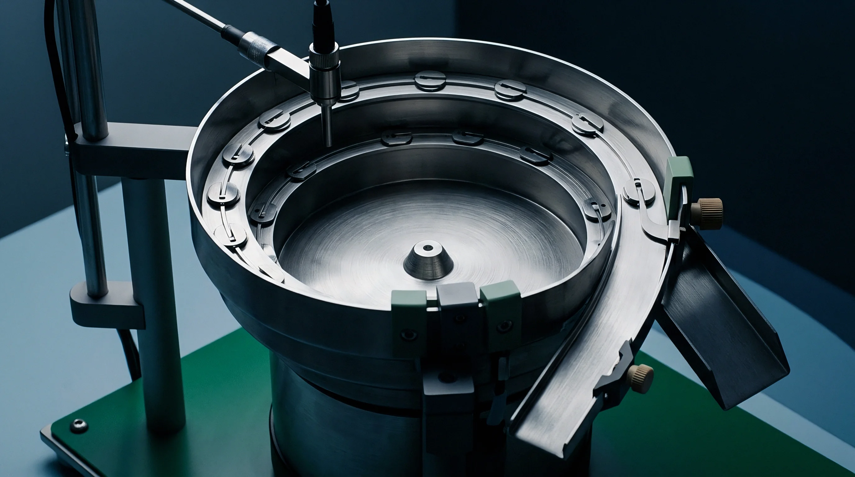
High-frequency ultrasonic energy focuses through piezoelectric lenses to concentrate acoustic pressure at target depth planes. Modern high-density interconnect substrates feature laser-drilled microvias with diameter dimensions ranging from 50 micrometers to 125 micrometers and dielectric layer thicknesses from 30 micrometers to 80 micrometers. Detecting interfacial delamination at the base of these microvias demands an acoustic focal spot size smaller than the diameter of the microvia target pad.
Acoustic focal spot diameter depends on the transducer center frequency, acoustic lens focal length, and the speed of sound in the fluid coupling bath. The lateral acoustic resolution follows diffraction-limited optical principles:
Spot Diameter = 1.02 (Focal Length Acoustic Velocity) / (Transducer Diameter Center Frequency)
A 230 megahertz transducer featuring a focal length of 4.3 millimeters and an acoustic aperture diameter of 3.0 millimeters yields a theoretical focal spot diameter of approximately 10.5 micrometers in water. This focal spot sits comfortably within the boundary of a 75 micrometer microvia capture pad. Operating at acoustic frequencies below 100 megahertz increases the focal spot diameter beyond 30 micrometers.
A focal spot larger than the microvia target pad averages acoustic energy across both the copper microvia post and the surrounding dielectric resin. Spatial acoustic averaging blurs the signal contrast, masking localized target pad delamination and allowing latent manufacturing defects to enter assembly production lines.
Inadequate acoustic focal alignment leads directly to missed target pad separations, passing defective high-density interconnect boards through initial inspection only to experience catastrophic field failures during thermal stress exposure.


Phase
Radio-frequency waveforms retrieved from interior board layers carry structural information within their polarity structure. Time-domain acoustic microscopy converts captured radio-frequency return signals into individual A-scan oscillograms. Every impedance transition inside the printed circuit board stackup produces an acoustic pulse peak on the A-scan timeline.
The arrival time of the pulse indicates the depth of the interface, while the phase orientation of the pulse confirms the physical change in acoustic impedance.

RF Signal Analysis for Interfacial Separation
Time-domain reflectometry measurements capture echo pulse sequences reflected from embedded microvia structures. When an acoustic pulse travels through a lower-impedance dielectric material and strikes a higher-impedance copper target pad, the reflected wave maintains the same phase orientation as the incident pulse. The initial echo peak points upward on the radio-frequency display, representing a positive reflection coefficient.
When the acoustic wave encounters an interfacial delamination or void gap at the copper boundary, the wave transitions from a higher-impedance medium into a lower-impedance gas medium. This physical condition forces a 180-degree phase shift in the reflected acoustic wave. The radio-frequency echo peak inverts, pointing sharply downward on the oscilloscope display.
A positive reflection peak signifies a transition to a higher acoustic impedance material, whereas a negative peak confirms an interfacial void or delamination.
Phase inversion detection algorithms analyze the raw radio-frequency echo data point by point across the gated microvia depth window. Software gates target the precise arrival time corresponding to the microvia base level, typically within a tight window of 2 to 5 nanoseconds. Phase-sensitive color mapping assigns bright red or white pixels to phase-inverted negative echo signals, while solid bonded interfaces render as grey or black background pixels.
Phase inversion identifies open interfaces.

What Spatial Resolution Isolates Microvia Base Separation?
Acoustic center frequencies between 230 megahertz and 400 megahertz deliver lateral spot sizes under fifteen micrometers. High-frequency acoustic energy suffers high attenuation in polymeric dielectric materials, limiting ultimate ultrasonic penetration depth. For microvias located in outer layers L1-L2 and L2-L3, 230 megahertz to 300 megahertz acoustic probes resolve delamination gaps with vertical separation distances as small as 10 to 20 nanometers.
Interfacial delamination at microvia target pads arises from distinct chemical and mechanical failure mechanisms during circuit board fabrication:
- Resin Smear Contamination occurs when mechanical or laser drilling leaves residual dielectric polymer on the internal target pad surface prior to desmear and electroless copper deposition.
- Interconnect Stress Cracking develops when thermal expansion forces tear the electrodeposited microvia copper post away from the underlying target pad contact interface.
- Target Pad Voiding forms due to incomplete electroless copper coverage, hydrogen gas entrapment, or fluid pocketing during initial wet processing operations.
- Black Pad Corrosion degrades electroless nickel immersion gold finishes on target pads, producing hyper-corroded nickel oxide surfaces that fail to form metallurgical copper bonds.
- Plating Seed Layer Separation emerges when severe mechanical stress causes micro-delamination between thin sputtered seed layers and bulk electrodeposited copper structures.
A sound signal reflecting from a solid copper interface maintains positive polarity, whereas a signal encountering a sub-micron separation gap flips phase entirely.


Probe
Scanning transducers transform high-voltage electrical excitation pulses into tightly bounded ultrasonic beam fronts. Transducer design balances acoustic operating frequency, focal length, transducer diameter, and lens material to optimize spatial resolution at specific microvia stackup depths. High-frequency acoustic scanning systems utilize quartz, sapphire, or specialized glass acoustic lenses bonded to zinc oxide or lithium niobate piezoelectric elements.

Frequency Selection and Focal Spot Diameter
Acoustic center frequencies determine the physical limit of lateral feature discrimination inside dense multilayer laminates. Select a 100 megahertz acoustic transducer when evaluating microvias situated deep within thick substrate structures where acoustic attenuation prevents higher frequencies from penetrating. Select a 230 megahertz or 300 megahertz transducer when analyzing fine-pitch high-density interconnect microvias in outer HDI build-up layers.
Focal depth governs interfacial signal clarity. Operating at higher acoustic frequencies enhances spatial resolution but severely reduces penetration depth through polymer resins and copper foil layers. High-frequency acoustic waves experience exponential attenuation during propagation through printed circuit board dielectrics.
| Center Frequency (MHz) | Focal Length in Water (mm) | Spot Size (-6dB) (µm) | Depth Penetration in FR-4 (µm) | Minimum Detectable Separation (nm) |
|---|---|---|---|---|
| 100 | 12.0 | 35.0 | 1200 | 100 |
| 140 | 8.0 | 22.0 | 800 | 50 |
| 230 | 4.3 | 10.5 | 350 | 15 |
| 300 | 3.0 | 7.5 | 200 | 10 |
| 400 | 2.0 | 5.0 | 90 | 5 |

Attenuative Losses in Fluid Media
Deionized water acts as an efficient transmission medium, yet high ultrasonic frequencies lose signal amplitude rapidly during fluid propagation. The attenuation coefficient of acoustic energy in water scales quadratically with frequency:
Attenuation (dB/cm) = 2.17 10^-4 (Frequency in MHz)^2
At an acoustic center frequency of 300 megahertz, acoustic attenuation in the water path reaches approximately 19.5 dB per centimeter. Water purity affects acoustic velocity. Maintaining a short focal path length of 2.0 millimeters to 4.0 millimeters minimizes fluid absorption losses.
Temperature stabilization of the liquid immersion bath within plus or minus 0.5 degrees Celsius prevents acoustic velocity drift and maintains consistent signal focal depth during scan acquisition.
Compliance with IPC-TM-650 Method 2.6.22 mandates non-destructive acoustic evaluation prior to thermal stress cycling to establish baseline interfacial integrity.
A rigorous acoustic scanning setup follows a precise calibration sequence to ensure microvia interface isolation:
- Mount the printed circuit board substrate flat in the temperature-controlled deionized water immersion tank using planar clamping fixtures.
- Position the ultra-high frequency acoustic transducer over an unpopulated copper calibration pad on the top layer.
- Adjust the motorized Z-axis stage to focus the acoustic beam precisely on the top copper surface to maximize the primary radio-frequency reflection peak.
- Lower the focus plane into the substrate by calculating the focal shift based on the refractive index ratio between water and dielectric laminate.
- Align the time-domain data gate to isolate the specific microvia target pad interface arrival time window.
- Set the analog-to-digital converter sampling rate to a minimum of 2.0 gigasamples per second to preserve high-frequency pulse shape details.
- Execute an X-Y raster scan over the microvia array at a step size equal to half the acoustic focal spot diameter.
Fabrication suppliers often claim that microvia target pad separation calls during acoustic scanning represent false positives caused by local resin weave variations. However, phase inversion signatures from air gaps provide unambiguous physical proof that cannot be mimicked by solid laminate weave structures.

Screening
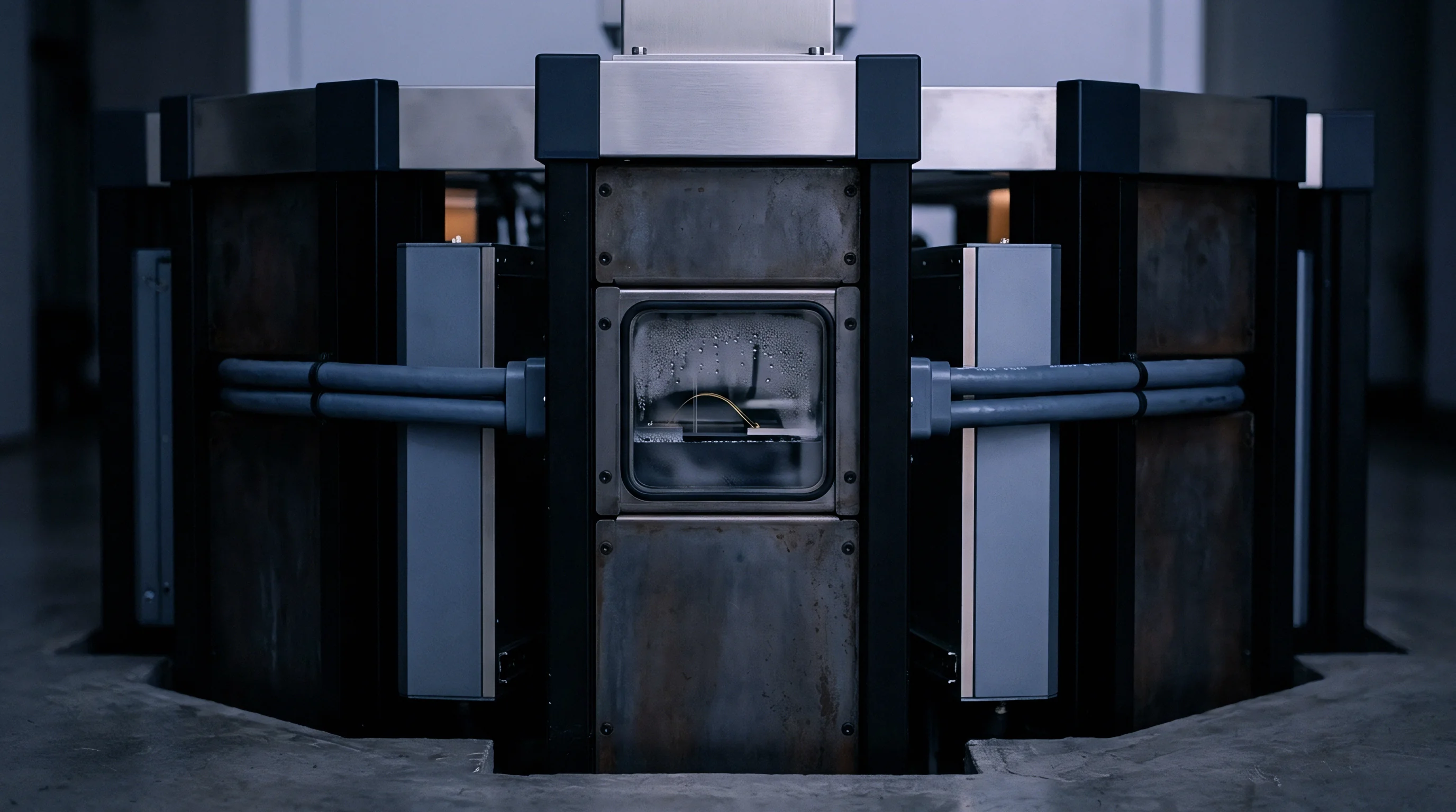
Environmental stress testing exposes weak mechanical interfaces before printed circuit boards enter assembly operations. Unstressed microvias featuring marginal metallurgical bonds or residual resin smear often pass initial electrical continuity tests and low-frequency acoustic inspections. Exposing boards to simulated assembly reflow thermal profiles drives mechanical stress into microvia structures, causing marginal interfaces to expand into full physical delaminations.
Thermal Stress Cycling and Delamination Propagation
Temperature excursions generate intense shear stress along material boundaries due to coefficient of thermal expansion mismatches. Electrodeposited copper exhibits a coefficient of thermal expansion of approximately 17 parts per million per degree Celsius. Unreinforced dielectric resins exhibit out-of-plane, vertical Z-axis coefficients of thermal expansion ranging from 50 to 250 parts per million per degree Celsius above their glass transition temperature.
Reflow heat expands trapped resin moisture. During lead-free reflow soldering, temperatures reach peak levels between 245 and 260 degrees Celsius. The intense vertical thermal expansion of the dielectric material pulls the target pad away from the microvia post.
If the metallurgical bond between the microvia base and the target pad lacks sufficient shear strength, the interface fractures.
Acoustic microscopy detects sub-micron interfacial gaps long before electrical continuity testing registers an open circuit.
Microvia target pad smear attenuates reflected waves. Early-stage interfacial cracking creates sub-micron gaps that allow intermittent electrical contact at room temperature while causing high-resistance open circuits at elevated operating temperatures. Non-destructive acoustic scanning performed after one, three, and six simulated reflow cycles catches latent delamination propagation before boards move to component assembly.

Interconnect Stress Test Correlation
Direct electrical resistance tracking during rapid thermal cycling identifies circuit path ruptures. Interconnect Stress Test coupons incorporate daisy-chained microvia structures subjected to cyclic DC current heating up to 150 degrees Celsius. Combining Interconnect Stress Testing with high-frequency acoustic microscopy establishes precise defect propagation rates.
When evaluating HDI substrate batches for acceptance, inspectors follow a strict decision criteria checklist:
- Phase Shift Analysis verifies whether returning radio-frequency waveforms display negative polarity inversion across any portion of the microvia target pad area.
- Acoustic Amplitude Mapping flags any target pad interface echo amplitude that exceeds 50 percent of the total input pulse signal level.
- Delamination Area Thresholds reject any individual microvia exhibiting interfacial separation over more than 15 percent of its total target pad surface area.
- Cluster Defect Criteria mandate lot rejection if more than 0.5 percent of microvias within a high-density grid display acoustic phase anomalies.
- Post-Thermal Growth Limits evaluate whether total delaminated area increases by more than 5 percent following three consecutive lead-free reflow stress cycles.
Thermal shock accelerates interfacial separation. Inspecting microvias with high-frequency acoustic microscopy before and after thermal stress screening isolates stable structural bonds from latent failure candidates. Unchecked microvias fail under mechanical stress.
What structural modifications inside the microvia plating process can completely eliminate target pad separation under extreme multi-pass lead-free reflow conditions?


Dossier
High-reliability manufacturing procurement contracts demand verifiable proof of structural integrity before batch acceptance. Relying solely on cross-sectional microsectioning leaves volume production lots exposed to destructive sampling limitations. Microsectioning destroys the sample while inspecting fewer than 0.001 percent of the microvias on a panel.
High-frequency acoustic scanning microscopy provides full 100 percent non-destructive coverage across every microvia target pad in a high-density interconnect panel layout.

Conformity Documentation for HDI Microvia Batches
Quality assurance archives require complete acoustic scanning datasets, microsection correlations, and lot trace reports. The technical compliance file accompanying shipped HDI substrate batches carries key evidence demonstrating interface structural integrity. Standard post-fabrication electrical continuity testing fails to detect partial target pad delaminations or marginal interfacial bonds.
Latent defects bypass electrical continuity checks.
A comprehensive acoustic verification dossier for an HDI board lot includes specific raw data and analysis records:
| Inspection Parameter | IPC Class 2 (General) | IPC Class 3 (High Reliability) | IPC Class 3/A (Space / Military) |
|---|---|---|---|
| Acoustic Transducer Frequency | Minimum 100 MHz | Minimum 230 MHz | Minimum 230 MHz to 300 MHz |
| Target Pad Phase Inversion Limit | Max 10% area per via | 0% phase inversion allowed | 0% phase inversion allowed |
| Post-Reflow Stress Screening | 3 Reflow Cycles (260°C) | 6 Reflow Cycles (260°C) | 9 Reflow Cycles plus Thermal Shock |
| Microvia Sampling Lot Size | AQL 1.0 Level II | 100% Panel Scan (Critical Vias) | 100% Full Substrate Area Scan |
| Data File Retention Period | 3 Years minimum | 7 Years minimum | 15 Years minimum |

Acoustic Audit Requirements for High-Reliability Shipments
Incoming inspection protocols validate incoming lot shipments through non-destructive acoustic evaluation sampling. Purchasing specifications dictate that microvia interfacial delamination calls identified by high-frequency acoustic scanning trigger immediate batch holding status pending joint failure analysis. Acoustic evidence secures warranty claims.
When an acoustic audit reveals phase-inverted echoes at target pad interfaces on sample panels, the entire production lot remains quarantined. The financial risk of assembling expensive active component silicon onto defective HDI substrates far outweighs the minor cost of acoustic screening. Rejected lots remain on supplier balance sheets.
Delamination voids the acceptance certificate.
Under IPC-6012E Section 3.6.2.11, evidence of target pad separation exceeding specified planar area limits on acoustic scan reports constitutes an explicit structural rejection condition that obligates the board fabricator to replace the entire manufacturing batch at their own expense.