
Algorithmic Trace Etch Compensation Factors for High Density Multilayer Circuitry
Algorithmic trace etch compensation scales photolithographic Gerber artwork to neutralize chemical undercut and hold target trace cross-sections.
Algorithmic trace etch compensation scales photolithographic Gerber artwork to neutralize chemical undercut and hold target trace cross-sections.

Differential etch control in ultra-fine pitch packaging requires precise chemical selectivity and hydrodynamic boundary layer management to clear seed copper.

Etch factor quantification converts trapezoidal microstrip sidewall angles into accurate field solver inputs to prevent high-frequency impedance shifts.

Modified semi additive process stackups require ultra-thin copper seeds under three microns to achieve sub-twenty-micron traces with stable impedance.
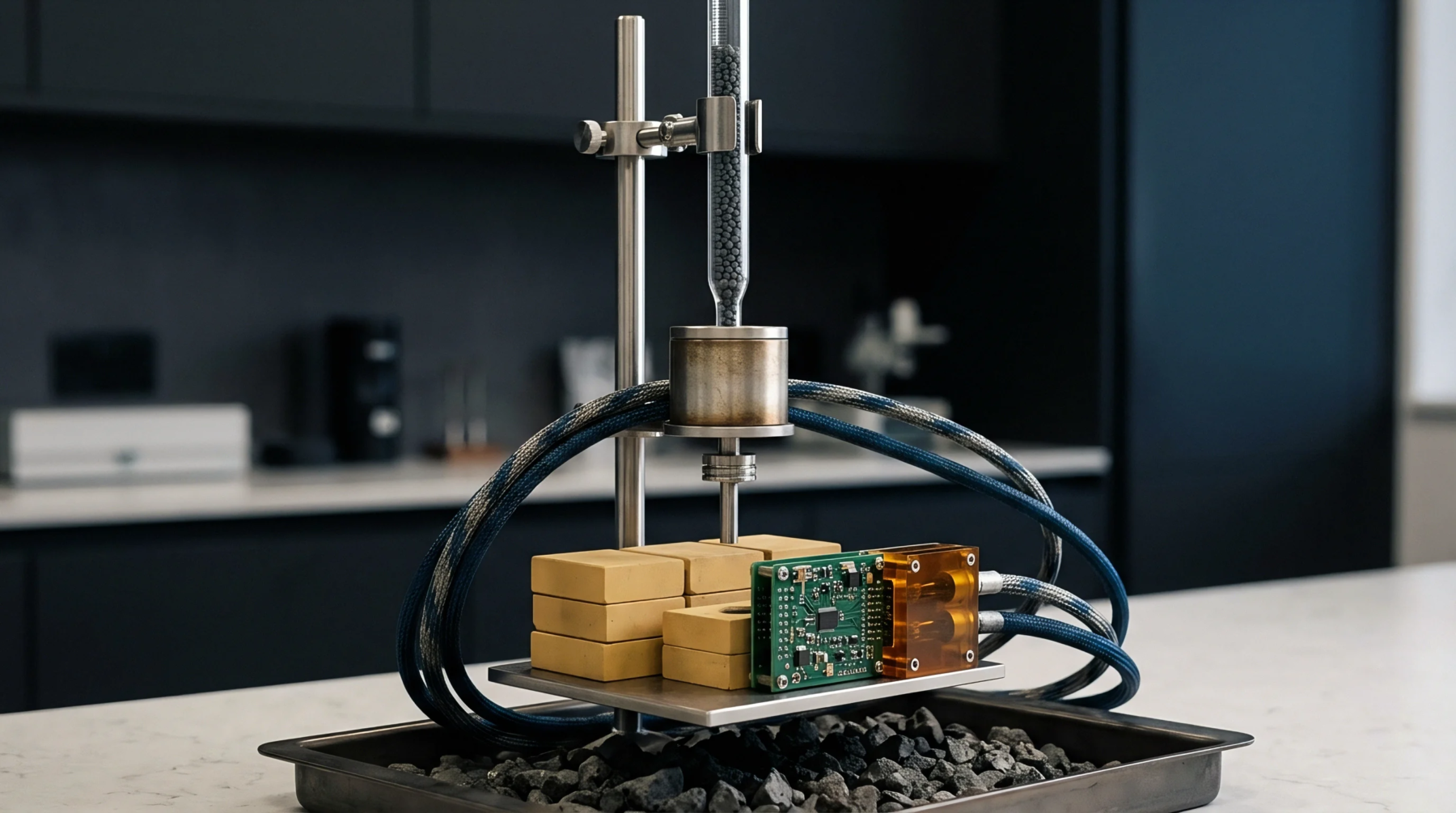
Controlling wet-process nozzle velocity below two meters per second prevents hydrodynamic trace stripping on ultra-thin inner layer copper channels.

Sub-50 micron trace etching demands mSAP seed layers, anisotropic chemistry passivators, and dynamic laser imaging scaling to hold 3.5+ etch factors and pass IPC Class 3 yield limits.
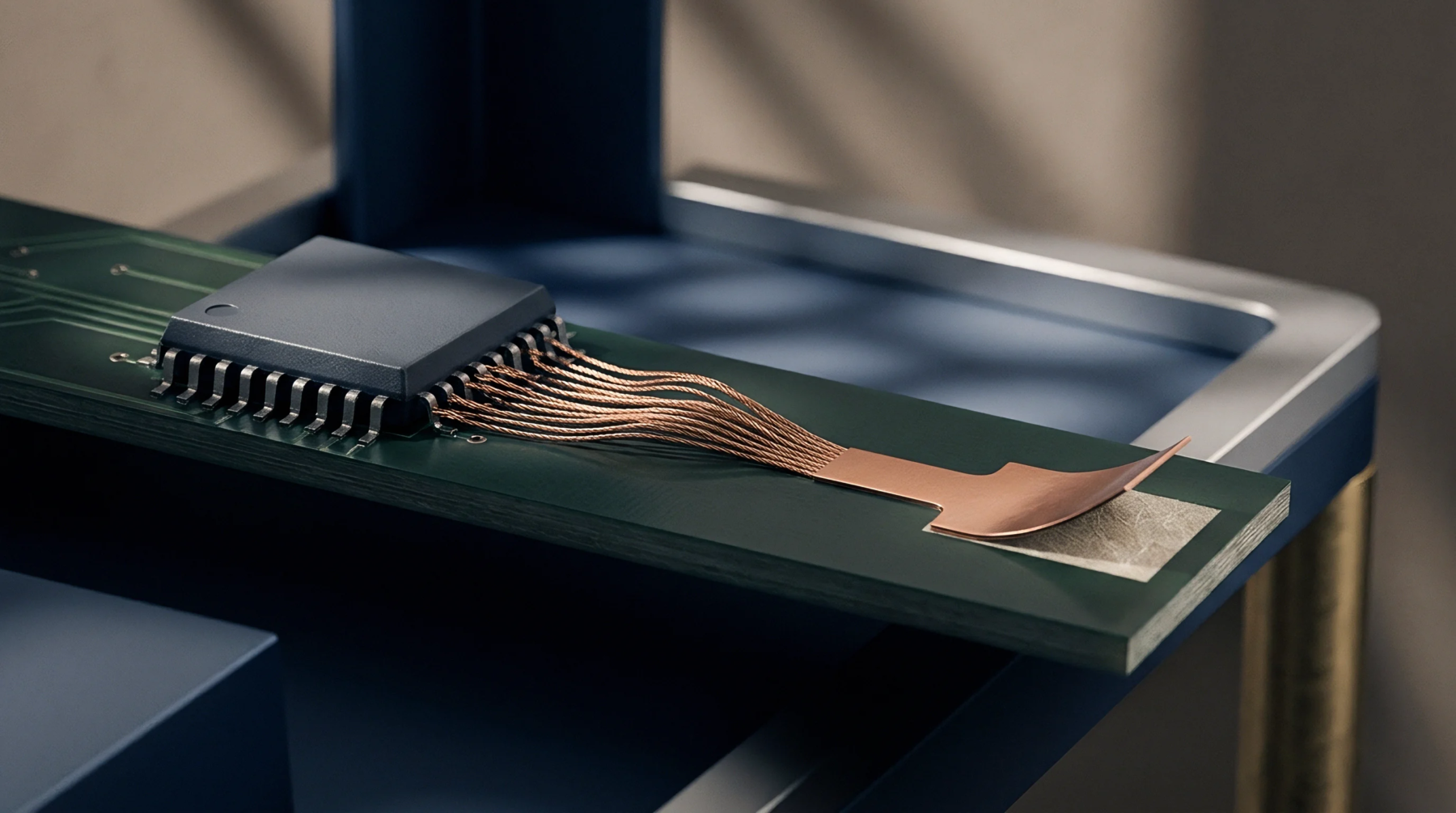
Sub-hundred-micron fine-line multi-core panel surcharges stem from seed-etch yield hits, core-shift registration buffers, and panel margin expansion.
Expertise is a utility, not a secret. sentiention™ publishes its working knowledge as open reference: intelligence layer covering the materials it sources, the markets it enters, and the reference that serves both.