Resolving Panel Edge Plating Current Density Variances in Automated Cross-Section Microstructural Reliability Testing
Resolving edge current density variances requires relocating coupons inward, applying dummy thieving patterns, and calibrating automated section optics.


Margin

Electric Field Collapse and Primary Density Divergence
Outer boundaries of a printed circuit panel act as electrodynamic field concentrators during electrolytic copper deposition. High potential gradients collect along panel edges, driving localized primary current densities to values two to three times greater than the panel center. In acid copper sulfate baths operating at nominal target current densities of 1.8 A/dm², outer coupons routinely experience localized rates exceeding 4.2 A/dm² without physical shielding.
This divergence alters the deposition kinetics within plated through-holes located on test strips positioned along outer tooling borders.
Secondary current density distribution attempts to moderate this primary concentration through electrochemical reaction kinetics. Polarizing additives, including suppressor polymers and organic bath accelerators, shift the Tafel slope by raising cathode overpotential at high-flux regions. Mass transfer limitations within small-aspect-ratio vias override this polarization effect when fluid agitation fails to replenish cupric ions at high deposition rates.
The resulting differential creates severe dog-boning, where copper thickness at hole knees on edge coupons exceeds center-hole barrel deposition by upwards of 65 percent.
Plating current density variations exceeding 1.2 A/dm² across panel borders alter copper grain structure from equiaxed to coarse columnar formations.

Microstructural Artifacts in Edge Test Coupons
Automated reliability testing relies on uniform coupon geometry to assess barrel fatigue, interconnect stress, and post-etch hole-wall integrity under IPC-TM-650 Method 2.6.8 thermal stress conditions. Excessively plated edge coupons yield misleading microstructural data during microsection analysis. Ductility drops significantly when elevated current density drives grain boundary elongation along the z-axis, altering tensile performance during thermal excursion testing.
Extremely high local deposition rates induce organic additive entrapment within the copper matrix. As current density surpasses the diffusion limit of brightener molecules, localized inclusions aggregate at grain boundaries, forming micro-voids during thermal stress testing. Automated optical metrology systems identify these void clusters as material flaws, masking the true reliability baseline of functional boards located inward from the perimeter.
| Panel Location | Nominal Current Density (A/dm²) | Hole Knee Thickness (µm) | Center Barrel Thickness (µm) | Dominant Grain Morphology |
|---|---|---|---|---|
| Outer Edge (Unshielded) | 4.1 | 48.2 | 24.1 | Coarse Columnar |
| Outer Edge (Thieved) | 2.3 | 33.5 | 27.8 | Mixed Equiaxed |
| Intermediate Zone | 1.9 | 29.1 | 28.0 | Fine Equiaxed |
| Panel Center | 1.7 | 27.4 | 26.9 | Fine Equiaxed |
Plating thickness disparities between edge test structures and interior array vias distort cross-sectioning results. When an automated polishing system prepares mounts containing edge coupons alongside interior structures, the differential copper removal rate produces uneven planar ground surfaces. Harder, thicker copper regions on edge coupons resist diamond slurry abrasives, causing specimen tilt that renders microsection measurements inaccurate.
Metallographic evaluation leaves unresolved whether peripheral current density corrections can be achieved purely through chemical polarization without modifying physical cathode border geometry.

Shield

Robber Bars and Dielectric Baffle Systems
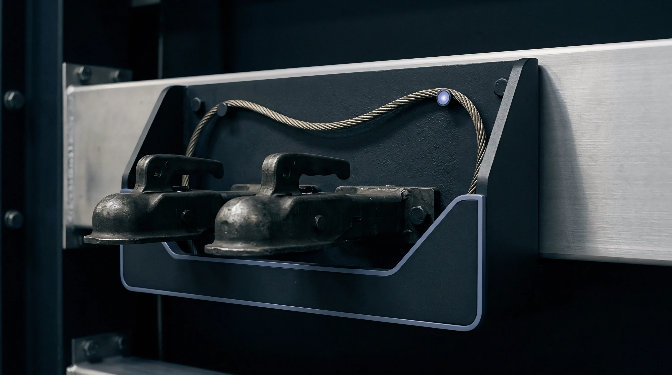
Cathode thieving structures alter the electric field geometry surrounding active panel areas. Solid copper thief borders placed 12 millimeters outside the outer coupon line draw excess current lines away from functional features. Incorporating thieving patterns on external panel frame borders drops peripheral current density down to within 12 percent of interior levels.
The thieving pattern must match the copper coverage density of adjacent functional circuitry to avoid creating secondary current sinks.
Dielectric shields mounted directly to plating racks block primary current lines without consuming copper anode material. Polypropylene baffles extending 50 millimeters inward from cathode frame edges re-route flux lines toward central panel regions. Optimizing baffle geometry balances the electric field across the entire cathode plane, suppressing edge over-plating while preventing center-hole starvation.

Hydrodynamic Fluid Delivery Integration
Solution agitation works in parallel with physical current shields to maintain microstructural equity across the panel surface. High-velocity sparger manifolds directing fluid perpendicular to panel surfaces strip the diffusion layer at hole entrances. Fluid replenishment inside edge-located vias reduces localized mass-transport polarization, ensuring additive consumption rates match the bulk electrolyte balance.
In impinging jet agitation cells, fluid velocity along outer panel margins frequently exceeds center-zone flow by 0.4 meters per second. Excessive local shear stress strips suppressor molecules from hole entries, allowing localized current spikes to recur despite physical thieving. Fabricators balance fluid dynamics by deploying eductor nozzles that equalize fluid velocity across the full panel span.
- Robber bar spacing requires placement within 8 to 15 millimeters of the outer coupon border to prevent field line leakage into active test structures.
- Segmented thieving grids prevent localized current concentration by utilizing 60 percent area-coverage dot matrices rather than solid copper borders.
- Baffle edge clearance must maintain a 25-millimeter offset from active coupon holes to avoid shadowing defects during electrodeposition cycles.
- Eductor flow velocity target ranges between 0.8 and 1.2 meters per second across panel faces to support uniform additive adsorption dynamics.
Correct placement of thieving elements keeps outer current densities inside acceptable processing windows.


Mount

Automated Sample Encapsulation and Planarization
Automated microsectioning equipment demands precise mechanical alignment to deliver reproducible coupon cross-sections. Epoxy encapsulation resins exhibit thermal expansion coefficients around 60 ppm/°C, contrasting sharply with the 17 ppm/°C expansion of copper metallization. When edge coupons carry excessively thick copper layers due to high current density, localized resin shrinkage during cure creates internal stresses that tilt the specimen mount.
Planar grinding of tilted resin mounts introduces structural distortion artifacts into automated optical measurements. Grinding wheels using 320-grit silicon carbide paper remove resin and thin copper at faster rates than the heavy copper knees of edge-located coupons. The resulting relief plane creates a false slope across the target hole barrel, altering the measured copper thickness by several micrometers.
IPC-6012 Class 3 acceptance mandates a minimum copper thickness of 20 micrometers across all hole wall microsections without structural relief tilt.

Polishing Mechanics and Optical Metrology Errors
Automated polishing routines utilizing 3-micrometer and 1-micrometer diamond suspensions exacerbate relief polishing around thick copper boundaries. Harder metallic features stand proud of the softer resin substrate. Optical auto-focus systems on microsection readers mistake rounding edges at the copper-resin interface for actual hole-wall boundaries, underreporting true plating thickness on over-plated coupons.
Varying copper area fractions within the cross-section mount alter polishing friction across the specimen face. Coupons harvested from unthieved panel edges present up to 40 percent higher copper surface areas than interior coupons. Automated equipment lacking dynamic pressure compensation applies uniform force across all mounts, resulting in under-polishing of high-density edge samples and over-polishing of sparse interior specimens.

What Causes Automated Readers to Flag False Barrel Cracks?
Optical microsection inspection software relies on edge-detection algorithms to locate copper-to-resin transition zones. Heavy relief rounding on over-plated edge coupons scatters incident light away from the microscope objective lens. The software interprets these dark, unlit relief shadows as physical cracks or micro-separations between the electroless copper seed layer and the electroplated barrel copper.
This optical artifact triggers automated lot rejections on coupons that possess complete structural integrity under manual tilt-light inspection.
Misaligned mounts generate systemic measurement errors across automated test runs. When resin abrasion rates diverge, automated sample preparation lines ruin entire test sets. Failure to normalize mount hardness across variable copper density coupons forces reliance on time-consuming manual cross-sectioning methods.

Discrepancy
Equiaxed Grain Formation versus Edge Columnar Growth
Electrodeposition at current densities below 2.0 A/dm² yields fine-grained equiaxed copper microstructures. Equiaxed grains accommodate thermal expansion stresses along the z-axis during solder reflow cycles through grain-boundary sliding. Under low current density conditions, organic brightener molecules adsorb evenly onto growing crystal faces, inhibiting preferential orientation and promoting isotropic mechanical properties.
High current density zones along panel edges alter the crystal growth regime toward columnar microstructures. When local flux exceeds 3.5 A/dm², copper ions deposit faster than organic additives can adsorb onto active crystal sites. Grains expand rapidly along the 111 crystallographic direction perpendicular to the hole wall, forming long, columnar columns with weak inter-columnar boundaries.
These weak boundaries act as preferred stress propagation paths during thermal shock testing.
| Current Density (A/dm²) | Tensile Strength (MPa) | Elongation at Fracture (%) | Grain Orientation Axis | Thermal Shock Cycles to Failure |
|---|---|---|---|---|
| 1.5 | 310 | 18.5 | Random (Equiaxed) | > 50 |
| 2.0 | 295 | 16.2 | Random (Equiaxed) | > 50 |
| 3.0 | 250 | 11.0 | Mixed (110 / 111) | 28 |
| 4.5 | 190 | 5.8 | Preferred (111 Columnar) | 11 |
Columnar copper structures exhibit low ductility under thermal stress conditions. When an edge-located coupon undergoes thermal stress per IPC-TM-650 Method 2.6.8, columnar grain boundaries fracture at significantly lower thermal cycle counts than equiaxed structures found in array vias. Automated testing systems flag these edge-coupon failures as representative of the entire panel, generating false reject signals for lots whose functional circuits contain sound equiaxed copper.
Grain boundary weakness correlates directly with elevated local current flux during electrodeposition. Suppliers frequently argue that edge coupon failure reflects extreme test severity rather than deficient plating bath control. Relying on uncorrected edge coupons leads to unnecessary scrap of acceptable production panels.


Correction

Coupon Relocation and Placement Matrix Optimization
Mitigating microstructural measurement variance requires repositioning reliability coupons within stabilized current density zones. Moving IPC-2221 target coupons inward by 25 millimeters places them inside the stabilized secondary current distribution area. Where panel space constraints force edge placement, fabricators must surround coupons with functional-density dummy thieving features to equalize local field intensity.
Panel design templates must enforce standardized current-density buffering rules across all production layouts. Incorporating thieving frames directly into CAD layer outputs eliminates operator discretion during panelization. The outer 15-millimeter perimeter of every production panel acts strictly as a sacrificial current-shielding border, excluding all test structures and functional circuits.
- Shift standard IPC-2221 microsection coupons inward by a minimum of 20 millimeters from the primary panel edge rout line.
- Fill all vacant outer frame area with copper thieving grids maintaining a 50 percent copper-to-dielectric ratio.
- Install physical polypropylene shielding baffles on plating racks to restrict high-angle electric field line convergence.
- Calibrate automated microsection polishing pressure based on measured metal surface area within the encapsulation mount.
- Apply optical shadow correction factors within automated cross-section inspection algorithms to account for minor edge relief rounding.

Mathematical Thickness Normalization and Yield Economics
Automated optical metrology systems can apply algorithmic correction factors to edge coupon measurements. By mapping the primary current field profile across a given panel geometry, software algorithms recalculate actual interior hole thickness based on edge coupon measurements. The model uses empirical deposition ratios to map measured edge knee thickness back to projected center-array values.
Consider an 18-layer high-reliability panel measuring 457 by 610 millimeters on 370HR mid-loss laminate, carrying an bare panel manufacturing cost of 320 USD per working board. A standard panel yields 4 working boards per frame. False lot rejections driven by unshielded edge coupon microsection failures destroy significant panel value.
Implementing calibrated thieving and automated measurement correction prevents non-conformance claims on acceptable production lots.
Standardizing current density controls across automated microsection workflows protects panel yield while maintaining IPC Class 3 structural compliance. Correcting electric field collapse at panel perimeters eliminates grain structure anomalies, aligns automated section prep with physical realities, and ensures microstructural testing reflects functional board quality accurately.