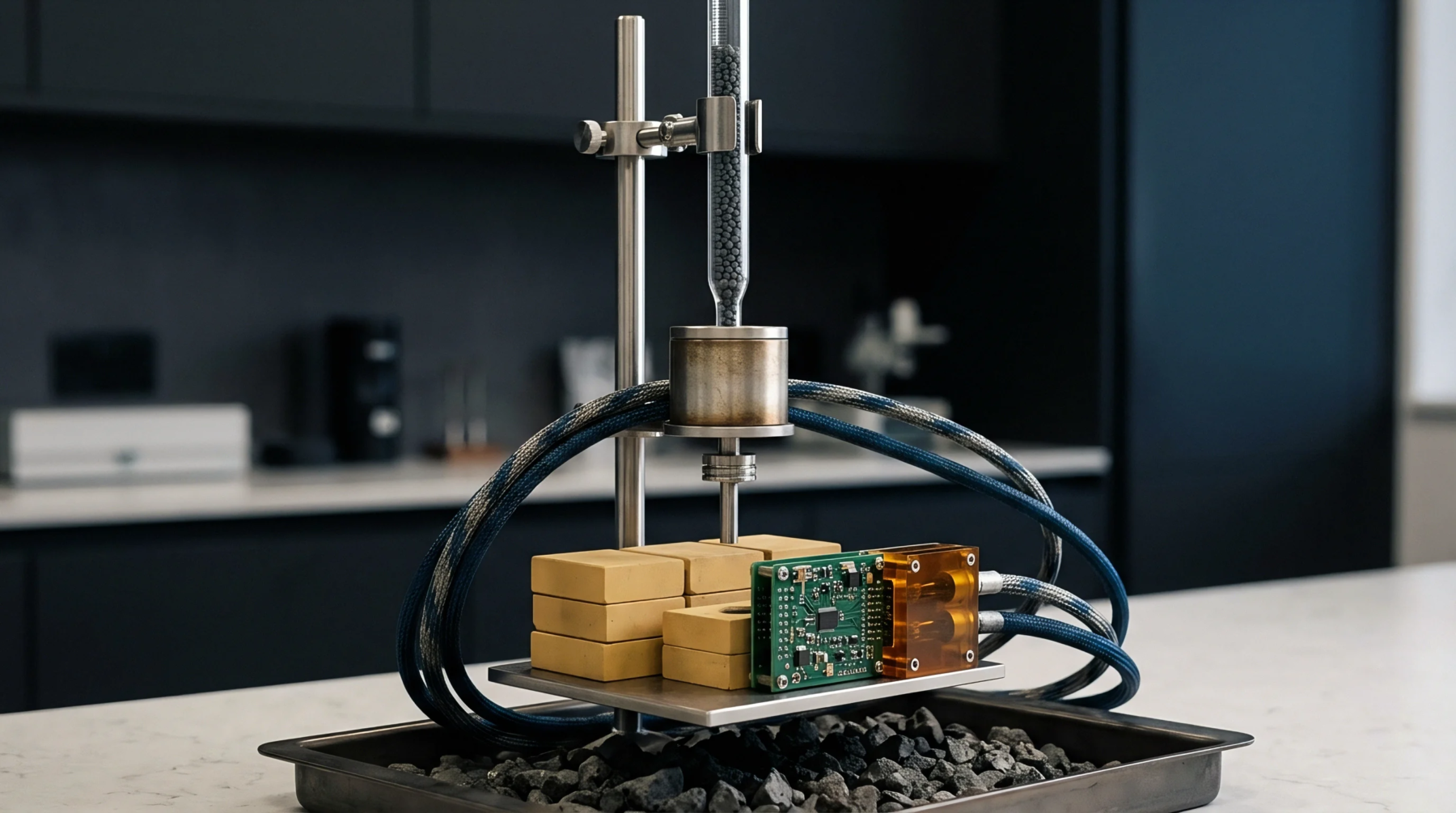
Thermomechanical Solder Joint Voiding Rate Effects on Long Term Field Failure Escape Probability
Interfacial solder joint voids accelerate creep strain accumulation, converting IPC-compliant connections into latent field open circuits.
Interfacial solder joint voids accelerate creep strain accumulation, converting IPC-compliant connections into latent field open circuits.
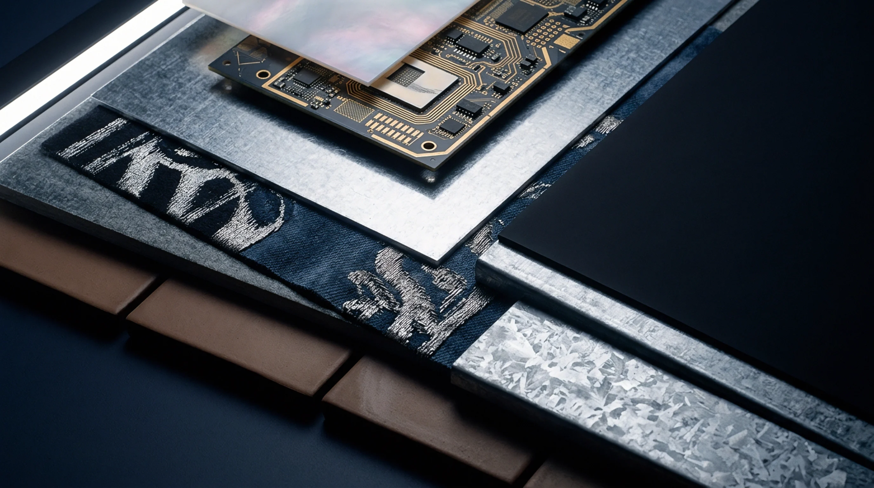
Micro BGA defect control requires qualifying stencil transfer efficiency, constraining machine placement landing force, and verifying joints via 3D laminography.
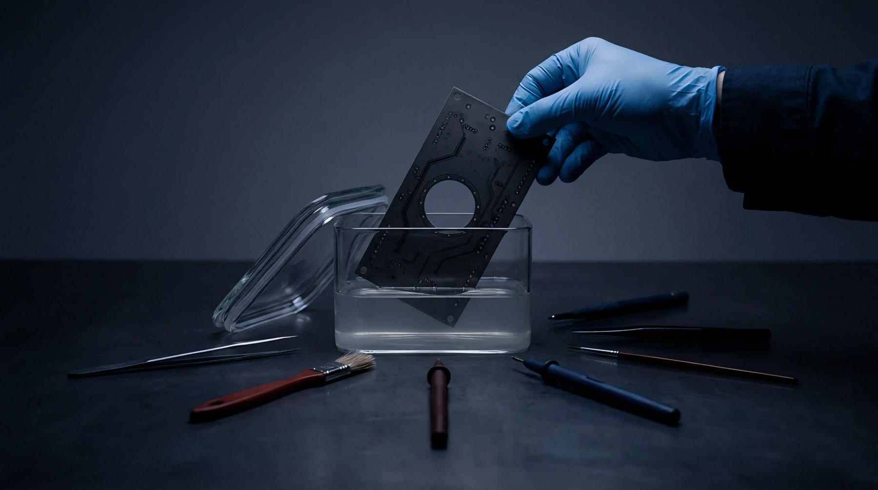
Secondary reflow coarsens lead-free solder microstructures and thickens interfacial intermetallics, cutting thermal cycling fatigue durability by up to 25 percent.
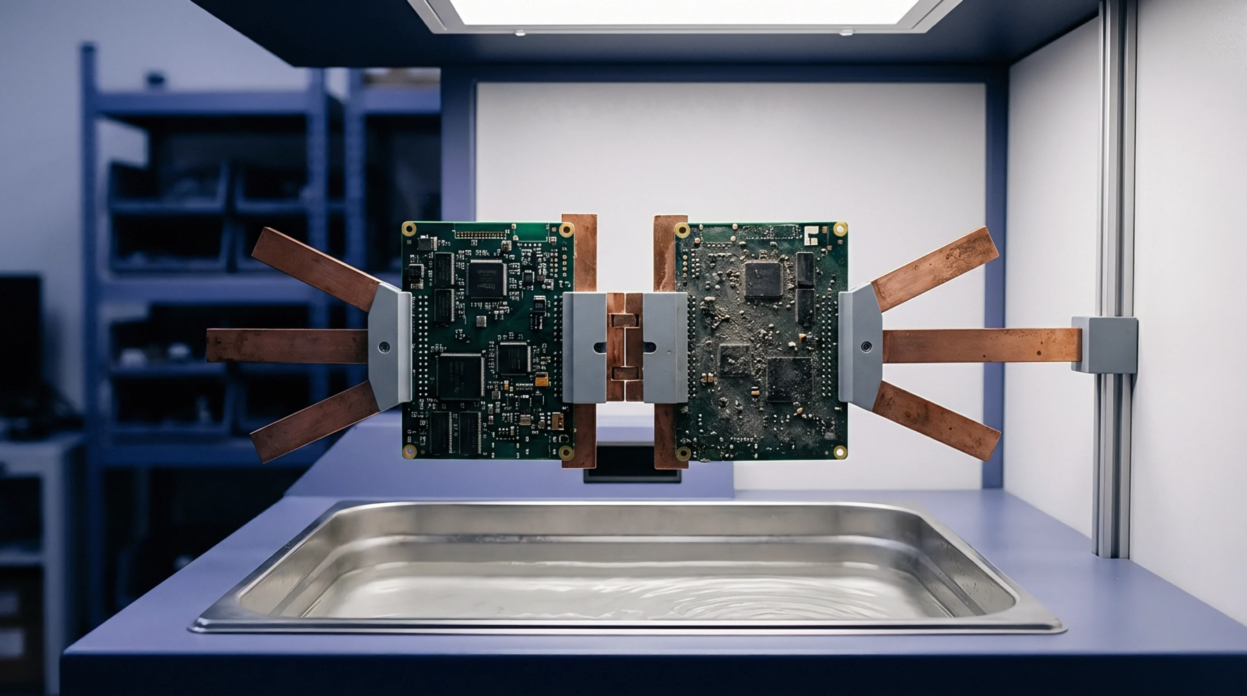
Additive nickel electroforming delivers mirror-smooth aperture walls and positive release tapers that preserve high-yield solder volume below 0.50 area ratios.
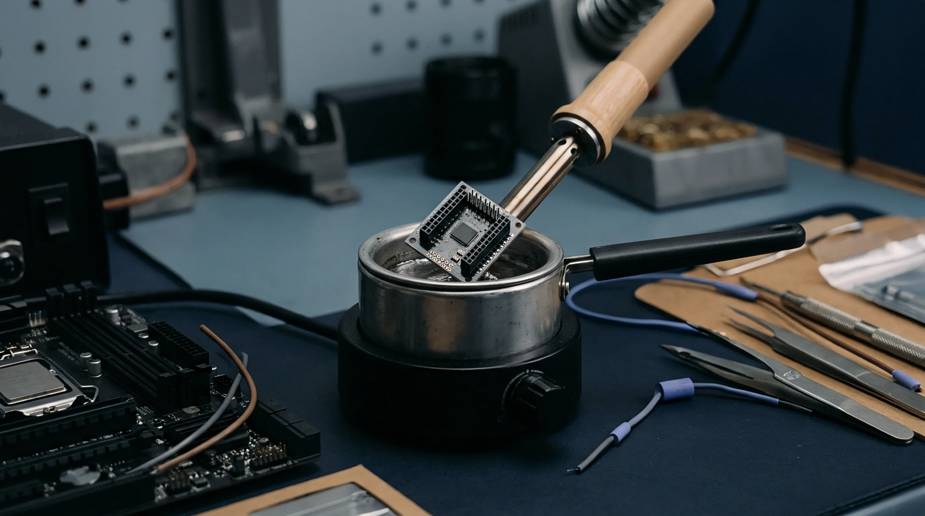
Calculate stencil area ratio above 0.66 for standard laser foil and above 0.50 for nano coated electroformed stencil to guarantee ninety percent paste release.
Designing component landing pads to standard fabrication tolerances ensures high panel yield, eliminates engineering queries, and stabilizes bare board unit costs.
Allocate micro BGA line standby and rework exposure by binding hourly downtime tariffs and hot-gas rework liability directly to SPI, AXI, and feeder logs.
Expertise is a utility, not a secret. sentiention™ publishes its working knowledge as open reference: intelligence layer covering the materials it sources, the markets it enters, and the reference that serves both.