Establishing Baseline SMT Stencil Area Ratios for Surface Mount Components
Baseline SMT stencil area ratios govern paste transfer efficiency, requiring minimum thresholds of 0.66 for standard foils and 0.50 for nano-coated apertures.
Baseline SMT stencil area ratios govern paste transfer efficiency, requiring minimum thresholds of 0.66 for standard foils and 0.50 for nano-coated apertures.

Optimize micro-pitch stencil area ratios above 0.50 by pairing fine-grain or electroformed foils, nano-coatings, and Type 5 paste to stabilize transfer volume.
Fine pitch SMT printing success relies on qualifying solder paste yield stress, thixotropic recovery, viscosity profiles, and tack retention dynamics.

Nano coated stencils sustain solder paste transfer efficiency above seventy-five percent across sub point six area ratios by reducing aperture wall friction.
Aspect ratios below 0.55 require electroformed or nanocoated foils and slow separation speeds below 0.2 mm/s to prevent wall friction starving solder deposits.

Type 5 solder pastes lower practical stencil area ratio limits from 0.66 down to 0.45 when paired with nanocoated or electroformed foils.

Dynamic thermal warpage pulls fine pitch arrays out of planarity during reflow; managing it requires stepped stencils, rigid pallets, and hot coplanarity data.

Sub-0.5 area ratios starve solder volume, accelerating brittle intermetallic boundary defects that require stepped stencils and Type 5 paste to resolve.
Additive nickel electroforming delivers mirror-smooth aperture walls and positive release tapers that preserve high-yield solder volume below 0.50 area ratios.
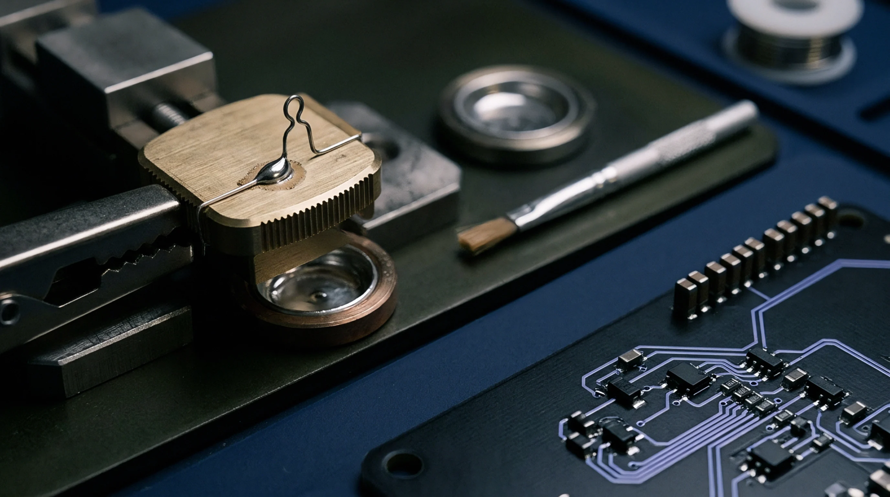
Aperture area ratios below 0.66 demand smooth sidewalls or nano-coatings to maintain 80 percent paste transfer efficiency.
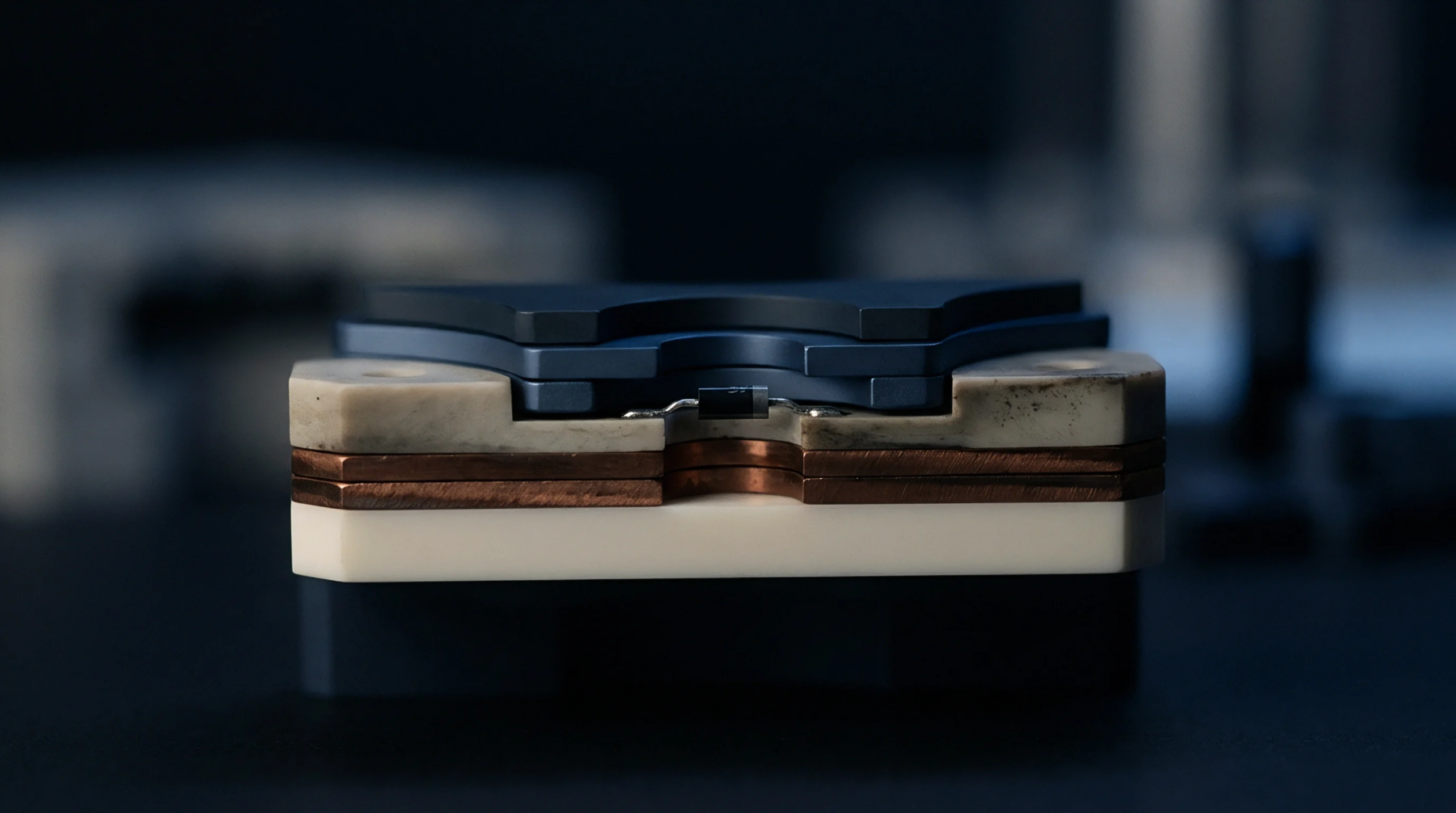
Micro-aperture solder paste transfer efficiency demands electroformed or nanocoated stencils, Type 5 powder, and strict 3D inspection controls below 0.55 area ratios.
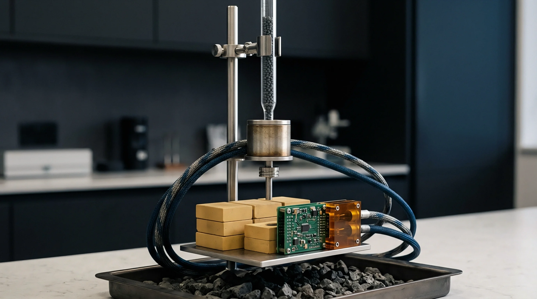
Optimize squeegee speed, separation rate, and aperture nanocoating to stabilize paste viscosity, maintain high transfer efficiency, and maximize SPI yields.
Verify stencil aperture area ratios exceed 0.66 using SPI volume data before adjusting reflow oven profiles for solder starvation defects.
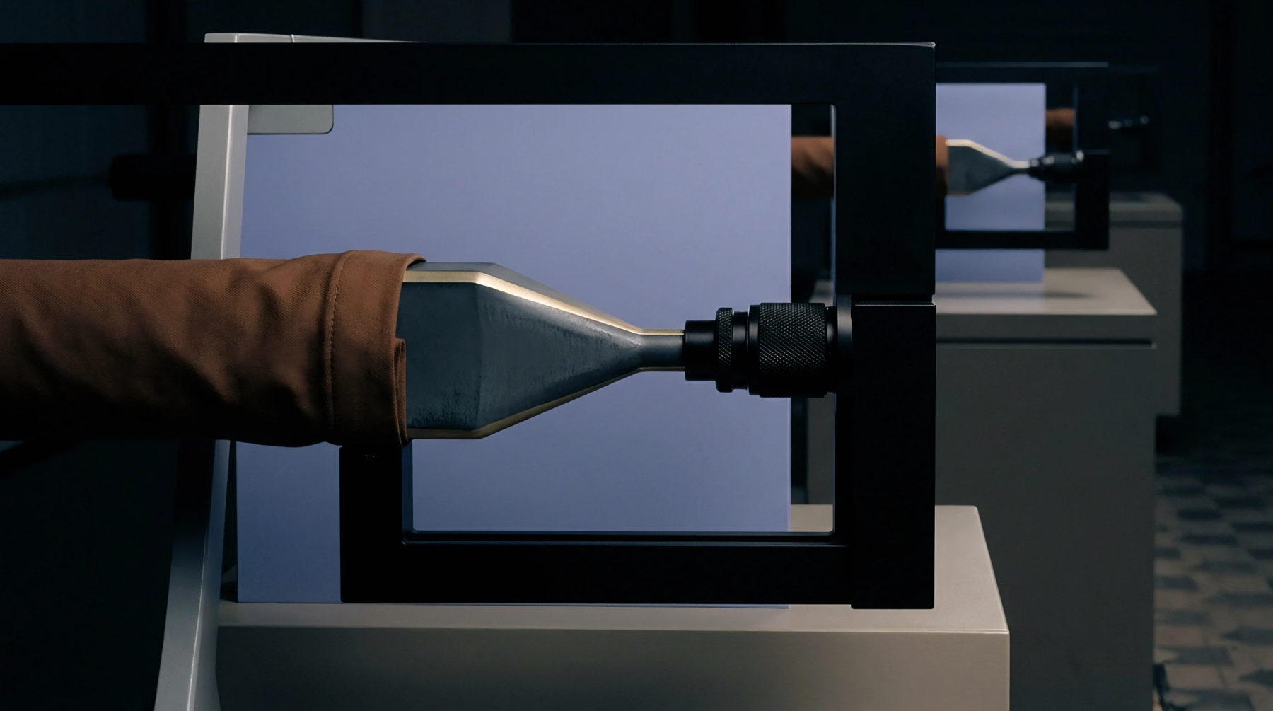
Allocate micro BGA line standby and rework exposure by binding hourly downtime tariffs and hot-gas rework liability directly to SPI, AXI, and feeder logs.

Electroformed nickel stencils lower aperture wall roughness below 0.08 µm Ra, enabling clean solder paste release at area ratios down to 0.50 for 0.3mm BGAs.

Verify SMT solder paste batches using Malcolm rotational viscometry and 3ITT rheology to prevent stencil slump, fine-pitch bridging, and volume transfer loss.
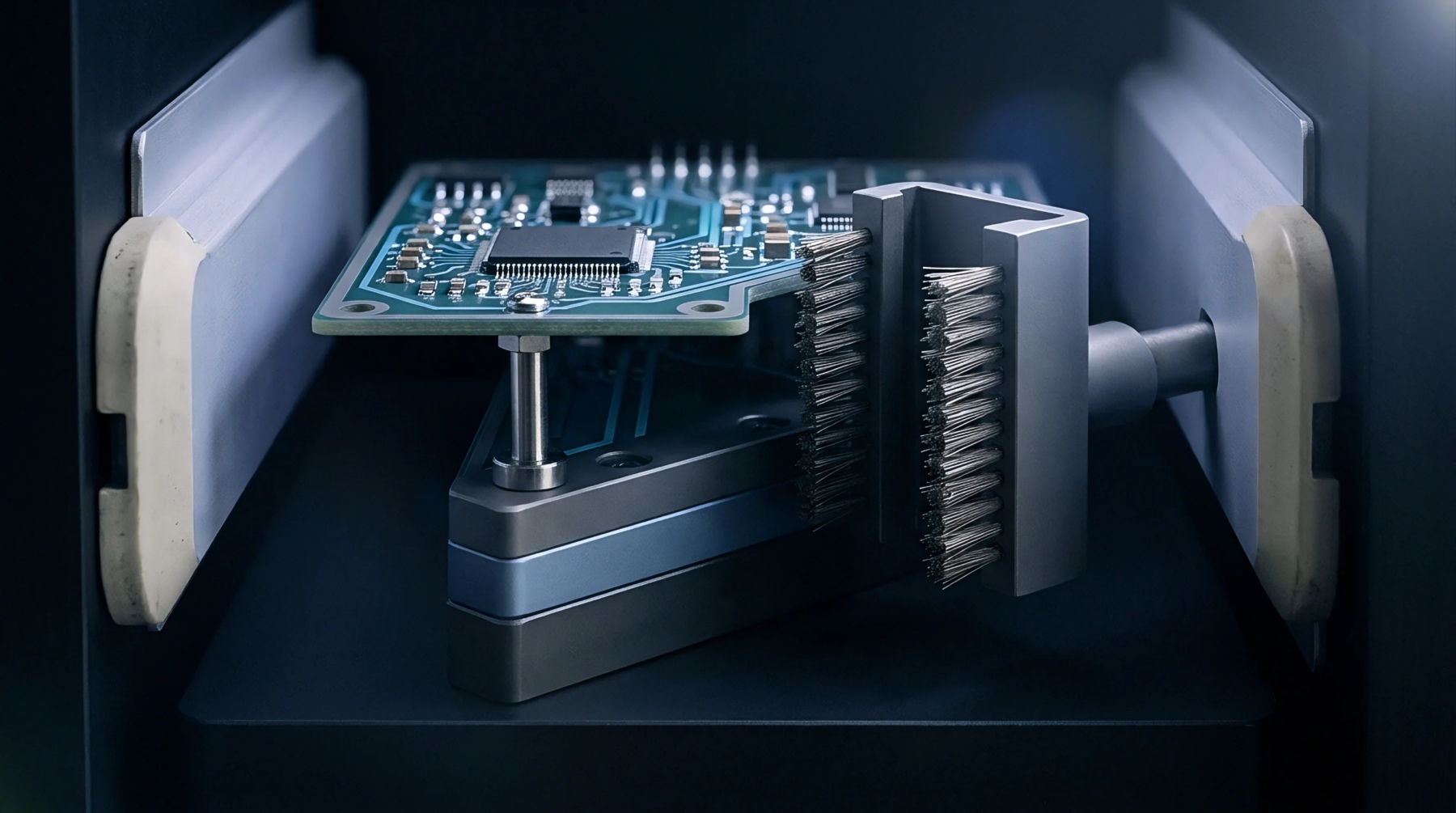
Component placement and soldering quality depend on stencil aperture ratios above 0.66, vision placement accuracy under 25 microns, and controlled liquidus reflow profiles.
Expertise is a utility, not a secret. sentiention™ publishes its working knowledge as open reference: intelligence layer covering the materials it sources, the markets it enters, and the reference that serves both.