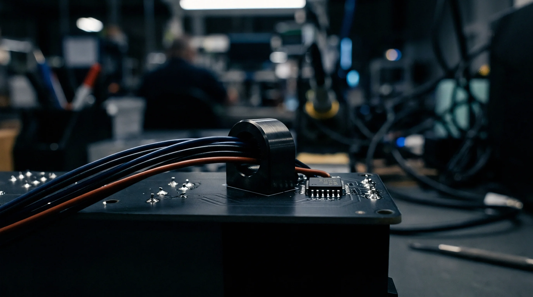
Probing Node
Dedicated copper landing features on a printed circuit board provide direct electrical interface for automated spring probes, flying probe heads, or boundary-scan connections. Designed into printed wiring layouts during board layout, a test access point translates schematic nodes into reachable physical targets for in-circuit test fixtures and diagnostic hardware. The target geometry permits automated electrical verification of passive component values, active device presence, and short-circuit conditions across trace paths.
Without planned contact landings, structural and electrical verification must rely on component leads, risking physical pad damage or intermittent measurement contacts during high-density manufacturing runs.
Layout Engineering
Physical test point geometries must adhere to rigid mechanical tolerances to maintain probing reliability across production batches. Dedicated circular or square pads typically range from 0.6 millimeters to 1.0 millimeter in diameter, permitting contact from standard spring-loaded pogo pins housed inside bed-of-nails test fixtures. Placement rules dictate minimum center-to-center pad spacing, generally targeted at 1.27 millimeters to 2.54 millimeters, which prevents mechanical interference between adjacent probe receptacles and sustains fixture strength.
Test targets located too close to tall surface-mount components suffer from shadowing, where the fixture press plate cannot drive the probe pin down without colliding with component packaging. Surface finish on the copper target directly affects contact resistance, with finishes such as Electroless Nickel Immersion Gold or Organic Solderability Preservatives showing distinct oxidation and wear profiles under repeated probe impacts. Repeated probe strikes with sharp crown, spear, or chisel tips deform the metal landing, breaking protective plating and introducing copper oxidation.
Via-in-pad geometries used as test nodes require flat, filled, and capped hole processing under IPC-4761 guidelines to prevent probe needles from slipping into open via holes and causing fixture misalignment.
Fixture Interface
Fabrication and assembly acceptance standards require high test target accessibility across all electrical nets. Full in-circuit test capability demands that every schematic net connect to at least one test access point, permitting comprehensive unpowered analog testing and node isolation. Where board density prevents complete net coverage, unprobed nets are shifted to boundary-scan testing or functional edge connector interfaces.
Probing accessibility metrics define final quality pass criteria prior to production release.