
Optimizing Bed of Nails Test Target Layout for in Circuit Testing
Positioning dedicated test targets on 1.0 millimeter centers with 0.8 millimeter target diameters maximizes first-pass in-circuit yield and prevents mechanical strain damage.
Positioning dedicated test targets on 1.0 millimeter centers with 0.8 millimeter target diameters maximizes first-pass in-circuit yield and prevents mechanical strain damage.

Test bead access on HDI substrates preserves microvia integrity during ICT while maintaining 98 percent node coverage when guided by precision fixtures.

In-circuit test layout requires minimum 28-mil test pads spaced on 50-mil centers, clear of component envelopes and balanced to prevent board flexure cracks.
Minimizing ICT solder joint fatigue requires triaxial strain gauge profiling below 500 microstrain at actuation speeds under 1,000 microstrain per second.
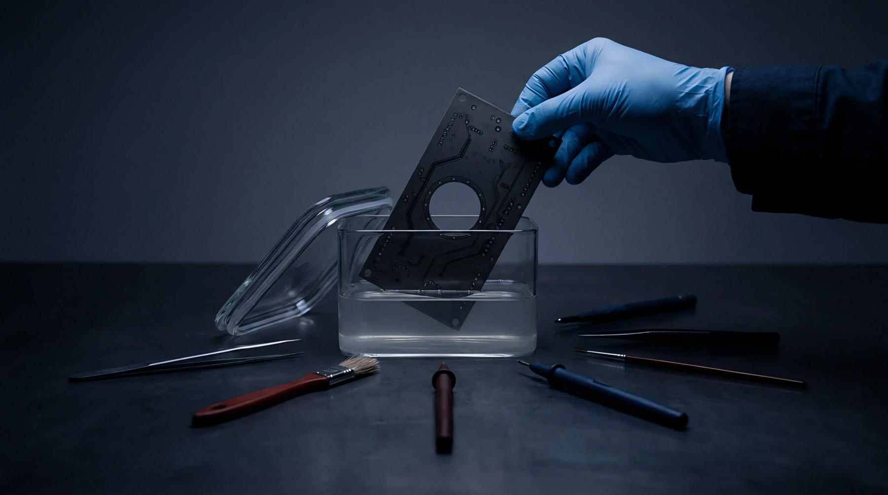
Balancing micro-probe forces with precision push-fingers prevents substrate strain over 500 microstrain, protecting fine-pitch BGAs and MLCCs from fixture damage.
Expertise is a utility, not a secret. sentiention™ publishes its working knowledge as open reference: intelligence layer covering the materials it sources, the markets it enters, and the reference that serves both.