Evaluating Plating Thickness and Microsection Coupons for High Reliability Purchasing
Plating thickness compliance demands precise coupon microsectioning to verify barrel copper, knee integrity, and innerlayer bonds against IPC standards.


Deposit
Minimum copper plating thickness in a through-hole marks the difference between reliable thermal cycling and early fatigue cracking. Standard fabrication routes deposit electrolytic copper onto hole walls made conductive by electroless copper or direct metallization. For high-reliability hardware governed by IPC-6012 Class 3 and Class 3/A, the barrel must survive ongoing thermal stress, mechanical vibration, and repeated assembly reflow cycles without structural compromise.
A finished copper barrel comprises two distinct deposits: a thin electroless seed layer followed by the electrolytic build. Evaluating barrel integrity requires checking both the average copper thickness along the hole wall and the absolute minimum at isolated thin spots. Because current density falls off toward the center of high-aspect-ratio holes, the mid-point of the barrel wall remains especially prone to light deposition.

Class Standards and Physical Metrics
Commercial boards built under IPC-6012 Class 2 call for an average hole-wall copper thickness of 20 micrometers, with localized thin spots allowed down to 18 micrometers. Class 3 tightens this to a 25-micrometer average and holds thin spots to at least 20 micrometers. Class 3/A, typical for space systems and demanding defense hardware, pushes the required average to 28 micrometers or higher, depending on contract master notes.
The transition where an outer pad meets the hole wall concentrates the electric field during plating. This current crowding draws copper preferentially to the surface, leaving the interior of the knee thin if bath additives ~ suppressors, levelers, and brighteners ~ fall out of balance. Microsection evaluations therefore check thickness at the surface, the knee, the barrel center, and internal land junctions.
| Specification Class | Average Hole Wall Copper | Minimum Thin-Spot Copper | Minimum Surface Wrap Copper | Minimum Cap Plating Thickness |
|---|---|---|---|---|
| IPC-6012 Class 2 | 20 μm (0.79 mil) | 18 μm (0.71 mil) | 5 μm (0.20 mil) | 12 μm (0.47 mil) |
| IPC-6012 Class 3 | 25 μm (0.98 mil) | 20 μm (0.79 mil) | 12 μm (0.47 mil) | 12 μm (0.47 mil) |
| IPC-6012 Class 3/A | 28 μm (1.10 mil) | 25 μm (0.98 mil) | 15 μm (0.59 mil) | 15 μm (0.59 mil) |
Wrap plating extends electrolytic copper from the barrel onto the outer surface land or inner wrap junction, keeping blind vias and wrap structures from pulling apart under z-axis thermal expansion. Under IPC-6012 Class 3, surface wrap copper must measure at least 12 micrometers over the base foil to ensure continuous metallization across the corner profile.
Cap plating seals filled vias in via-in-pad designs with electrodeposited copper. A planar cap lets solder balls or surface-mount leads seat evenly over buried holes without outgassing or solder voiding. Cross-sections must confirm that cap thickness meets drawing minimums without showing subterranean voids or resin sink-back beneath the copper.
Writing IPC-6012 Class 3 requirements directly into fabrication master notes turns general quality expectations into clear, enforceable criteria for lot acceptance and rejection.

Coupon
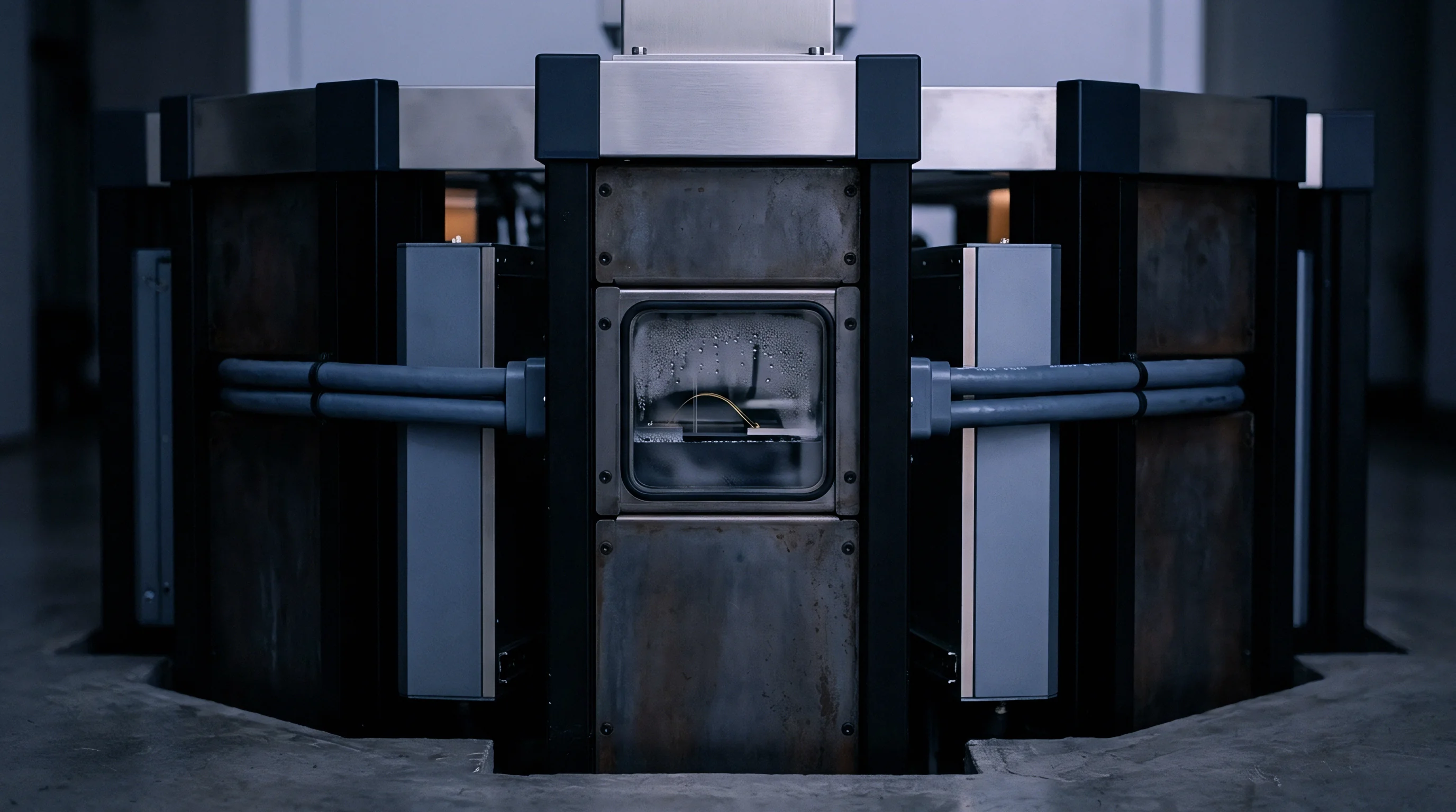
Sacrificial coupons placed along panel borders provide the primary physical means to verify bare-board integrity without cutting into production circuits. Fabricators lay out these test vehicles to duplicate the drill diameters, pad geometries, layer counts, and copper densities of the adjacent functional boards on the same manufacturing panel.
Test structures sitting near panel edges experience different plating bath hydrodynamics than features in the board interior. Surrounding coupons with solid borders or copper thieving prevents localized current spikes from driving up coupon plating thickness relative to functional circuits.

IPC Test Structure Classifications
IPC-2221 standardizes coupon designs by letter code, assigning each to evaluate specific physical or electrical characteristics across the panel.
| Designator | Feature Evaluated | Primary Microsection Focus | Target Defect Mechanism |
|---|---|---|---|
| Coupon A | Plated Through-Holes (PTH) | Hole wall copper thickness, knee copper, barrel integrity | Thin wall copper, hole voids, microcracks |
| Coupon B | Surface Insulation & Resistance | Trace spacing, surface contamination, dielectric insulation | Electromigration, ionic contamination |
| Coupon C | Registration & Etchback | Innerlayer land-to-hole alignment, hole etchback depth | Misregistration, drill smear, resin wicking |
| Coupon D | Interconnect Stress & Thermal Shock | Daisy-chain hole series under repeated reflow simulation | Innerlayer separation, barrel fatigue failure |
| Coupon E | Controlled Impedance | Trace geometry, dielectric thickness, etch profile | Impedance deviation, trapezoidal trace erosion |
Coupons must see the exact thermal and chemical sequence applied to the production panel. Inspectors use Coupon A and Coupon B to check barrel plating, inner-layer registration, and the adequacy of post-etch cleaning. Coupon D routes a continuous daisy chain for four-wire Kelvin resistance measurements before and after thermal conditioning; any resistance jump flags micro-cracking or inner-layer separation well before physical cracking shows externally.
Coupons positioned strictly along panel edges can exhibit thicker plating than board centers unless copper thieving balances local current density.
Sound practice places coupons at opposing corners or along opposite mid-edges of every panel. On multi-up arrays, procurement specifications typically require at least two microsection coupons per panel to capture edge-to-center plating variations. High-reliability contracts generally require these coupons to remain attached to the working panel until incoming inspection or metallographic analysis is formally signed off.
Coupons isolated from surrounding copper patterns draw localized current spikes, yielding thickness measurements that misrepresent the functional circuits.

Specimen
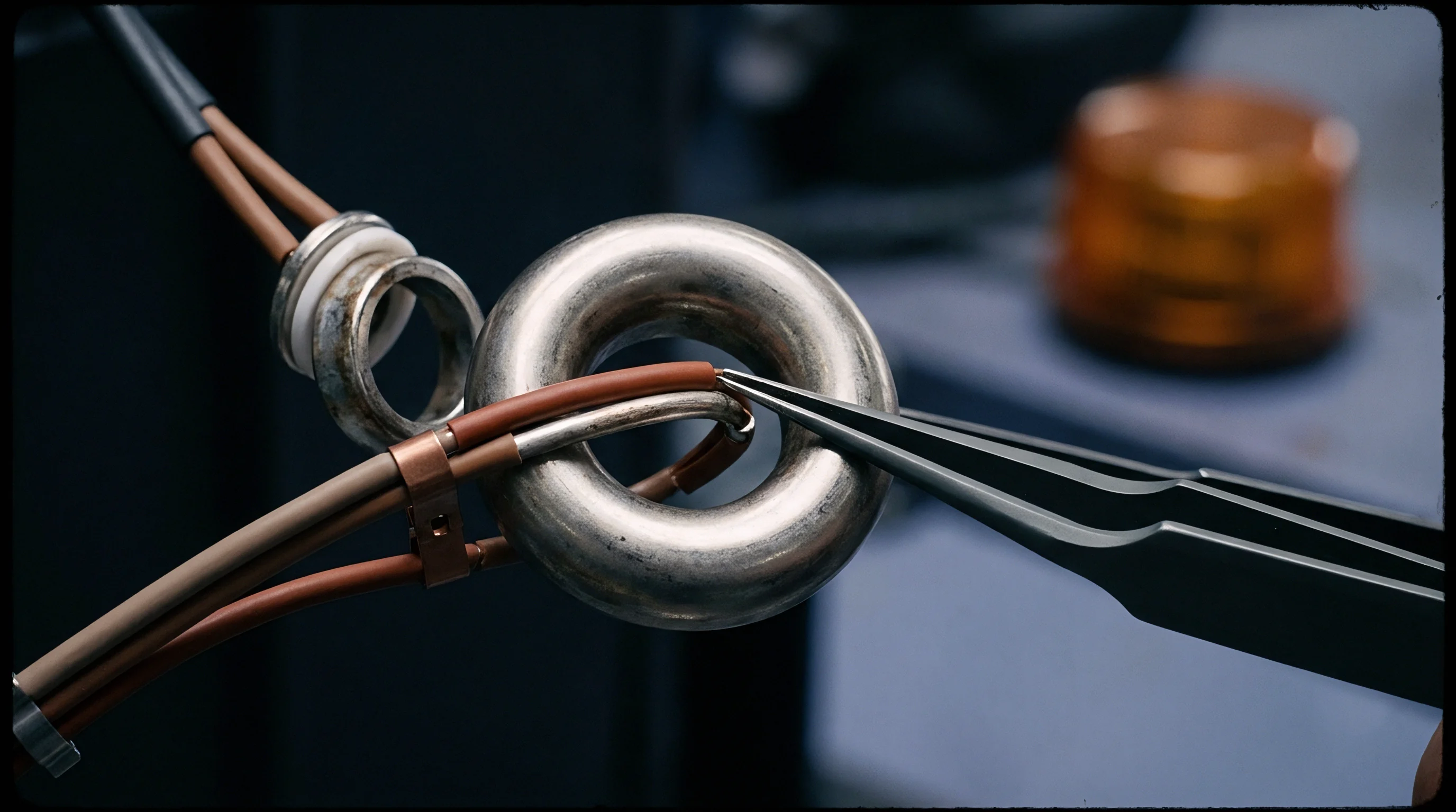
Preparing microsection mounts requires disciplined grinding, encapsulation, and polishing to prevent edge rounding and artificial copper smear. Preparation begins by cutting the coupon from the panel with a low-speed diamond saw or precision router, avoiding mechanical shocks that could damage plated hole walls.
Encapsulation relies on cold-curing epoxy systems formulated for low exotherm and minimal shrinkage. Acrylic resins set faster but generate curing temperatures high enough to induce thermal stress or resin recession in heat-sensitive base materials. A low-viscosity epoxy penetrates fine voids and stabilizes internal copper layers through subsequent grinding.

Grinding and Polishing Protocol
Mechanical preparation follows a staged abrasive sequence, working through silicon carbide papers before moving to diamond slurries on non-woven cloths.
- Coarse planar grinding uses 240-grit to 450-grit silicon carbide paper under water lubrication to bring the preparation plane close to the hole centerline.
- Fine grinding refinement advances through 600-grit and 1200-grit papers to eliminate coarse scratches and remove subsurface deformation.
- Primary diamond polishing uses a 3-micrometer diamond suspension on hard synthetic cloth to keep the copper-dielectric boundary flat and unrounded.
- Final oxide polishing applies a 0.05-micrometer colloidal silica or alumina suspension on a soft nap cloth to clear remaining sub-micron scratches and yield a mirror finish.
Keeping the mount parallel during grinding ensures the polish plane bisects the true centerline of the barrel. Grinding off-center overstates copper wall thickness through geometric projection errors.

How Does Micro-Etching Expose Copper Grain Structure?
Chemical micro-etching strips away the smeared copper layer left by mechanical polishing, exposing grain boundaries, plating interfaces, and intermetallic layers. Ammonia-based formulations and ammonium persulfate solutions attack grain boundaries selectively without pitting the surface.
| Reagent Chemistry | Active Composition | Etch Duration | Target Structural Feature Revealed |
|---|---|---|---|
| Ammonium Hydroxide / Hydrogen Peroxide | 50 mL NH4OH, 50 mL H2O2 (3%), 50 mL H2O | 3 to 8 seconds | Electrolytic copper grain structure, plating joins |
| Ammonium Persulfate | 10 g (NH4)2S2O8 in 100 mL H2O | 5 to 10 seconds | Recrystallization, boundary separation, electroless interface |
| Micro-Etch Chromic Acid | 5 g CrO3, 0.5 g Na2SO4, 100 mL H2O | 2 to 5 seconds | Intermetallic boundary layers, nickel-copper interfaces |
Micro-etching distinguishes the fine, equiaxed structure of ductile electrolytic copper from columnar or coarse deposits that crack readily under thermal expansion. The etch also clarifies transitions between base foil, electroless seed, electroplated barrel copper, and cap deposits.
Microsection preparation must achieve a centerline cut within 10 percent of the actual drill radius to avoid geometric measurement distortion.
Reported copper separation frequently reflects underlying lamination bond failure rather than damage introduced by microsection preparation.


Fracture
Plated hole walls fracture during assembly reflow when thermal expansion stress exceeds the tensile strength of the electrodeposited copper. Dielectric laminates expand along the z-axis at six to eight times the rate of the surrounding copper barrel, imposing severe tensile strain on the plated wall, inner-layer joints, and outer knees.
Anomalies found in cross-sections trace directly to base laminate properties, drilling parameters, desmear thoroughness, and plating chemistry balance.
- Barrel cracking splits the central span of the plated hole wall where z-axis expansion generates maximum tensile strain during reflow.
- Knee fracture parts the copper at the corner radius between the surface pad and hole wall under concentrated stress.
- Innerlayer interconnect separation pulls internal lands away from the plated barrel, usually caused by drill smear or inadequate desmear etchback.
- Resin recession leaves gaps between the outer barrel wall and cured dielectric, driven by outgassing or incomplete resin wetting during lamination.
- Nodular plating creates irregular copper bumps on the hole wall, seeded by particulates in the plating bath or inadequate filtration.
- Etchback wicking draws plating chemistry down glass fiber bundles along the drilled wall, eroding internal dielectric clearances.
Chemical desmear uses permanganate or plasma processes to strip resin smear from internal copper lands before electroless seeding. IPC-6012 Class 3 permits positive etchback to give three-sided contact to internal lands, but rejects negative etchback that leaves internal copper edges recessed behind the dielectric hole wall.

Aspect Ratio and Current Density Calculations
A through-hole’s aspect ratio governs solution exchange and local current density through the barrel during plating. Higher aspect ratios restrict fluid circulation, starving the center of the hole of copper ions.
For a 1.6 mm thick board drilled at 0.25 mm diameter, aspect ratio is:
Aspect Ratio = fracBoard ThicknessDrill Diameter = frac1.6 mm0.25 mm = 6.4:1
In an electroplating bath operating at a surface current density of Jsurface = 2.5 A/dm2, fluid resistance inside a 6.4:1 hole drops the effective current density at the center to roughly Jcenter = 1.6 A/dm2. By Faraday’s law of electrolysis, deposited copper mass m scales directly with current density and plating duration t:
m = fracM · I · tz · F
Here M is the atomic weight of copper (63.55 g/mol), z is the valence state (+2 for cupric ions), and F is Faraday’s constant (96,485 C/mol). Because local current I drops toward the center of a high-aspect-ratio hole, plating thickness decreases accordingly. When 60 minutes of plating yields 32 micrometers on the surface, mid-barrel thickness drops to:
Thicknesscenter = 32μm × left(frac1.6 A/dm22.5 A/dm2right) = 20.48μm
This 20.48-micrometer result borders on the 20-micrometer minimum for Class 3. If bath leveling additives fall short, mid-barrel thickness easily dips below specification, causing panel rejection during coupon cross-sectioning.
Solder float conditioning at 288 degrees Celsius for 10 seconds induces Z-axis expansion stress that exposes weak innerlayer interconnect joins.
Plating voids stem from trapped air bubbles, residual drill debris, or outgassing during electroless seeding. IPC-6012 Class 3 allows no microvoids in structural wrap zones and restricts barrel voids to isolated occurrences covering no more than 5 percent of the total wall length.
Undetected inner-layer separations frequently pass room-temperature continuity testing, then open intermittently under field thermal cycling.

Dossier
Receiving documentation must correlate directly with submitted test pieces to verify that thermal stress conditioning occurred before microsectioning. Auditors verify that cross-section reports document the specific pre-conditioning cycles applied before potting and grinding.
Production shipment documentation packages must include specific objective quality records:
- Certificate of Conformance signed by quality authority, affirming compliance with drawing notes, the approved stackup, and designated IPC class rules.
- Thermal stress log recording pre-bake schedules, solder pot temperatures, and float durations (typically 288°C for 10 seconds per IPC-TM-650 2.1.1).
- Microsection optical micrographs showing plated barrel cross-sections at 100x and 200x magnification with calibrated scale bars.
- Dimensional measurement sheet detailing measured copper thickness at the surface, knee, and mid-barrel for each evaluated coupon.
- Ionic contamination test report confirming that extract conductivity indicates less than 1.56 micrograms of NaCl equivalent per square centimeter.
Microsection reports without calibrated scale bars or alignment indicators do not provide verifiable proof of conformance. Receiving inspection requires etched grain structures in photographs; un-etched, as-polished copper can easily conceal micro-cracks and inner-layer separations.
Cross-referencing panel coupon serial numbers against fabrication batch logs prevents sub-standard test structures from validating high-reliability lots.
Whether non-destructive X-ray fluorescence can fully substitute for destructive coupon cross-sectioning on high-frequency, low-loss laminates remains under active industry study.

Invoice
Unit pricing reflects panel utilization, coupon border allocations, and metallographic lab overhead. Accommodating a full IPC Class 3 coupon set takes 12 to 18 percent of panel border area, cutting into the live area available for circuit arrays and driving up bare-board costs.
Stepping from IPC-6012 Class 2 to Class 3 typically adds 15 to 30 percent to bare-board pricing, depending on layer count, aspect ratio, and laminate selection. The increase reflects slower plating tank throughput, tighter bath maintenance, lab labor for coupon evaluation, and yield fallout against minimum wall-thickness thresholds.
Purchase agreements should define which party covers re-sectioning when incoming inspection encounters borderline dimensions. Retention clauses require the fabricator to archive companion coupons for five to ten years, preserving physical evidence for root-cause analysis if field failures emerge later.
Clear scrap allowances and defined re-sectioning protocols protect high-reliability programs against arbitrary lot rejections while setting definite acceptance criteria for the shop floor.