
Evaluating Vectorless Test Sensor Attenuation in AC Coupled Gigabit Differential Traces
Vectorless test on AC coupled traces requires active guarding and stimulus tuning to overcome capacitive divider losses and detect open solder joints reliably.
Vectorless test on AC coupled traces requires active guarding and stimulus tuning to overcome capacitive divider losses and detect open solder joints reliably.

In-circuit testing cannot reliably detect BGA solder cracks because fixture pin pressure temporarily closes micro-fractures during electrical continuity scans.

Resolving boundary scan degradation above twenty megahertz requires controlled fifty-ohm routing, point-to-point buffering, and series damping to prevent ringing.
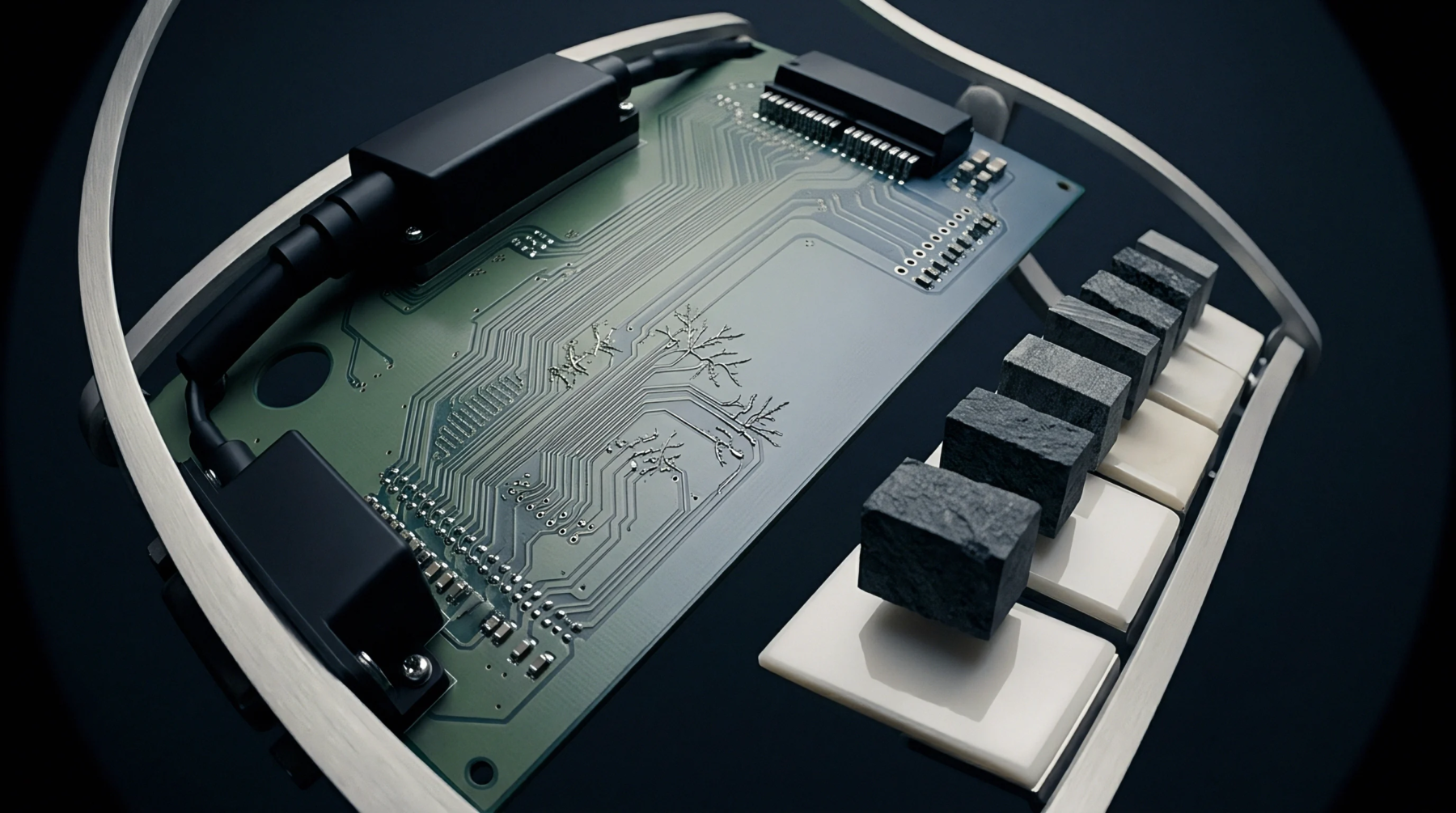
High-speed signal integrity degradation in hybrid boundary scan bed-of-nails testing is resolved by de-embedding fixture parasitics and shortening test stubs.

Combining boundary scan with bed of nails testing maximizes structural defect detection while reducing mechanical probe points and fixture maintenance costs.
Unprobed net fault escapes are quantified by combining physical nodal access constraints with statistical defect densities and secondary inspection regimes.

Positioning dedicated test targets on 1.0 millimeter centers with 0.8 millimeter target diameters maximizes first-pass in-circuit yield and prevents mechanical strain damage.

Proper test target placement ensures high structural fault coverage, prevents component damage, and reduces defect escapes in printed circuit assemblies.

Mathematical optimization of test node selection balances fault coverage against substrate micro-strain, preventing cumulative fatigue failure.
Evaluating dynamic inductive phase noise coupling in sub-millimeter boundary scan pins requires active phase noise spectrum checks during TCK clock shifting.

Amorphous electroless nickel crystallizes into Ni and brittle Ni3P above 310°C or via Sn diffusion during reflow, driving voiding and joint shear failure.

High-speed functional testing validates SerDes signal integrity via calibrated de-embedding, dynamic eye-margin capture, and tight thermal regulation.

IEEE 1149.6 pulse-based boundary scan screens AC-coupled differential SerDes channels for opens and shorts without physical test pads damaging signal integrity.

Reduced physical test access on microvia boards increases latent defect escape rates, requiring thermal stress screening and coupon cross-section verification.

Reducing physical test access on high-density interconnect circuit boards increases defect escape rates unless boundary scan and 3D X-ray vectors bridge the structural coverage gap.
Incomplete physical test access increases latent structural defect escape rates, requiring complementary boundary scan and X-ray testing to protect field reliability.

Optimizing test lands requires balancing parasitic capacitance below 0.15 pF with board strain limits under 500 micro-strain during in-circuit probing.
Combining boundary scan logic with flying probe readings narrows analog isolation boundaries, eliminating un-vectored physical test points while preserving milliohm accuracy.

Optimizing BGA nodal access requires balancing physical microvia test pads with IEEE 1149.1 boundary scan to maximize structural defect coverage.
IEEE 1149.6 boundary scan overcomes DC blocking in high speed differential pairs by evaluating edge transition pulses across embedded capacitive decoupling networks.

Hybrid regimes combine physical in-circuit probes for analog passives with IEEE 1149 boundary scan to close high-density BGA structural fault coverage gaps.

High density test point sizing requires balancing probe mechanical drift tolerance against board layout real estate to ensure reliable nodal coverage.

Boundary scan cell allocation dictates structural fault coverage by converting physical IC pins into software-driven stimulus and response registers.
Modified counting sequence vectors compress boundary scan runs to logarithmic depth, isolating micro-bridges and cracked solder joints before field exposure.
Phase-separated ground layers limit transient extraction through local dielectric polarization saturation and microvia current crowding under high di/dt loads.

Weibull shape parameters below unity reveal latent microstructural interface escapes that pass zero-hour electrical testing but fail under thermal stress.

Thermal fatigue in surface mount joints is driven by CTE mismatch creep and interfacial voiding, requiring event-detected thermal cycling to prevent field failure.

Integrating IEEE 1149.1 and 1149.6 boundary scan vectors recovers structural test coverage on unprobed nets, eliminating latent BGA solder escapes before shipment.
Expertise is a utility, not a secret. sentiention™ publishes its working knowledge as open reference: intelligence layer covering the materials it sources, the markets it enters, and the reference that serves both.