Matrix Suppression Corrections for Phthalate Quantification in Solder Masks
Correcting matrix suppression in solder mask phthalate testing requires isotopic dilution or standard addition to prevent false RoHS compliance passes.
Correcting matrix suppression in solder mask phthalate testing requires isotopic dilution or standard addition to prevent false RoHS compliance passes.

Interlaboratory calibration drift in Py-GC-MS flame retardant testing is controlled by setting guardbands that deduct expanded uncertainty from regulatory limits.
Calibrated solvent extraction recovery factors correct raw analytical residue mass, preventing unextracted organic flux contaminants from escaping batch qualification.
Setting guard bands per ISO/IEC Guide 98-4 at two standard uncertainties protects PVC screening from false RoHS compliance calls while limiting re-test rates.
Applying a guard band equal to expanded uncertainty creates an acceptance limit that eliminates false compliance declarations for polyvinyl chloride compounds.

Verify restricted phthalates in PVC wire insulation using solvent dissolution or thermal desorption GC-MS under IEC 62321-8 to ensure levels stay below 0.1%.
Solvent-induced flex circuit delamination occurs when processing chemicals depresses polymer transition temperatures and degrades interfacial work of adhesion.

Determining Flory-Huggins interaction parameters quantifies solvent sorption limits in polyimide flex insulation, preventing moisture-driven dielectric failure.

Solvent exposure plasticizes polyimide insulation, lowering dielectric strength up to seventy percent and requiring post-wash baking and Weibull lot auditing.

Unrecovered interface trap density extracted via sub-microsecond pulse testing provides the accurate, unannealed baseline needed for field lifetime projection.
Sub-7nm BTI modeling requires capturing ultrafast recovery and stochastic defect distributions to set accurate silicon timing margins and burn-in screens.
Standardized thermal burn-in methods accelerate silicon infant mortality through monitored thermal and voltage stresses to ensure field-grade reliability.
Quantifying activation energy dispersion and thermal gradients requires spatial thermal mapping and non-isothermal kinetics to prevent qualification lifetime errors.

Accelerated burn-in models life consumption by multiplying thermal Arrhenius ratios by field acceleration factors to purge infant flaws without exhausting oxide life.
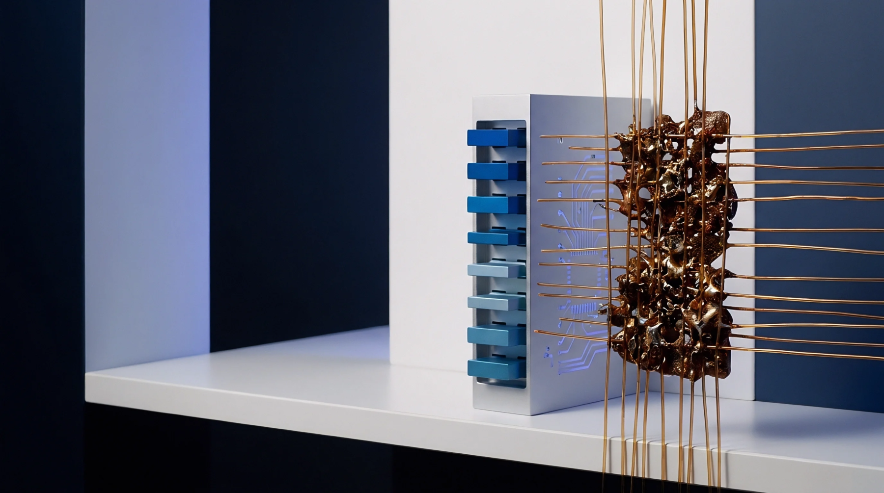
Thermal stress modeling translates package material thermal mismatches into precise accelerated life chamber profiles, preventing field fatigue escapes.
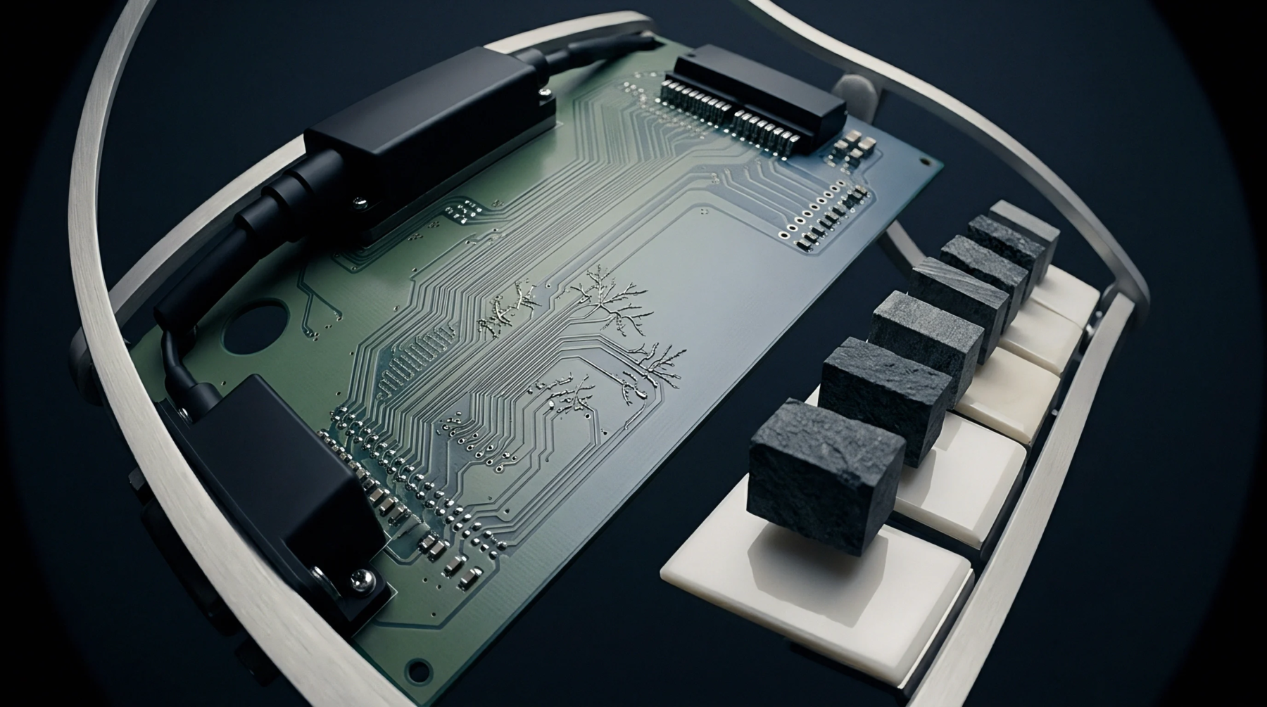
Quantify fatigue damage in low-temperature micro-alloy joints by extracting viscoplastic work from thermal profiles using calibrated Weibull wear-out data.
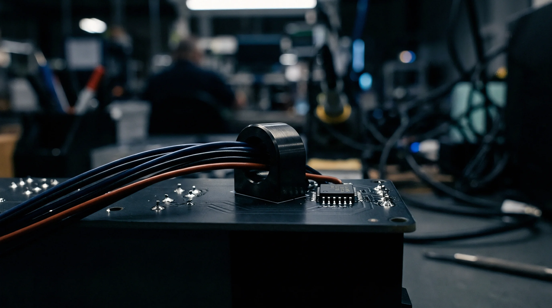
Palmgren-Miner fatigue calculations cap stress screening damage below five percent of endurance to preserve circuit assembly field reliability.
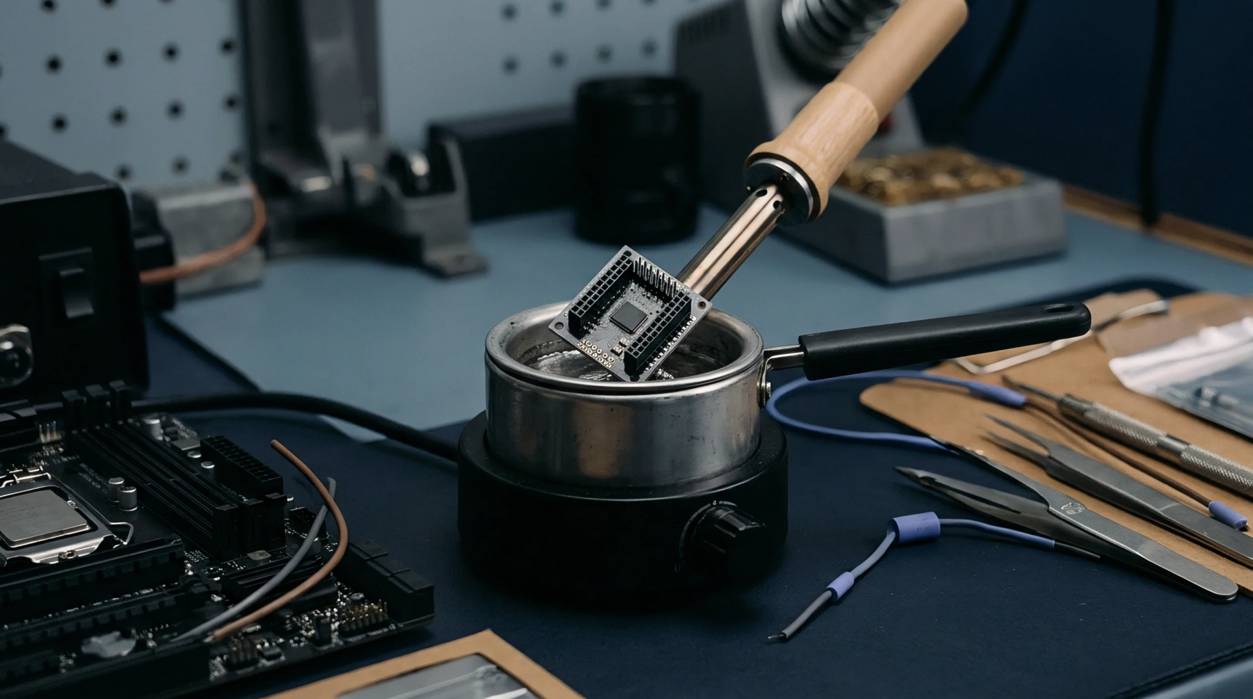
Calculate solder fatigue acceleration factors by pairing alloy creep kinetics with exact thermal profiles to prove assembly batch field survival.

Narrowing mass-to-charge transmission filters below twenty percent distribution width stops monomer recoil knock-in during cluster processing.

Quantifying cluster beam interface broadening requires isolating atomic mixing and roughness via MRI model deconvolution to prevent false lot rejections.
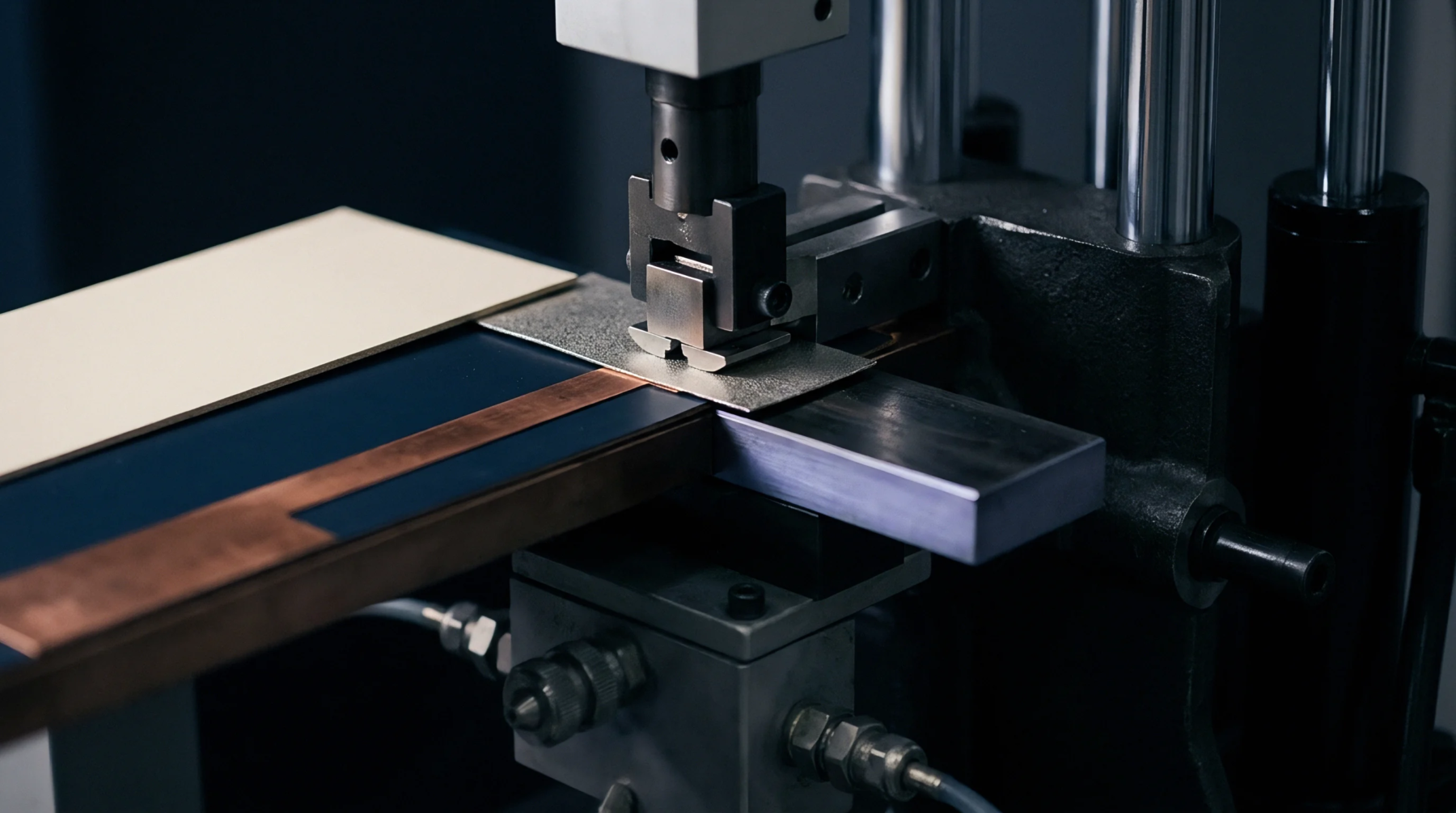
Cascade mixing deforms ultra-shallow SIMS profiles; low primary ion energy and MRI deconvolution restore true concentration profiles for wafer lot acceptance.

Mass filtered argon cluster beams achieve non-linear sputter yields by controlling energy per atom distributions to minimize subsurface damage during profiling.
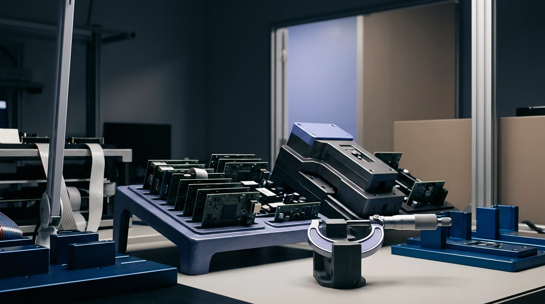
Gas cluster profiling controls surface damage by partitioning ion energy among thousands of atoms, preserving stoichiometry and interface sharpness.

Argon gas cluster beam sputter yield calibration requires precise step-edge profiling or quartz microbalance mass tracking under verified beam current suppression.
Field singularity extraction models predict high-frequency partial discharge inception by correlating microscopic trace edge radii with localized space charge ionization limits.
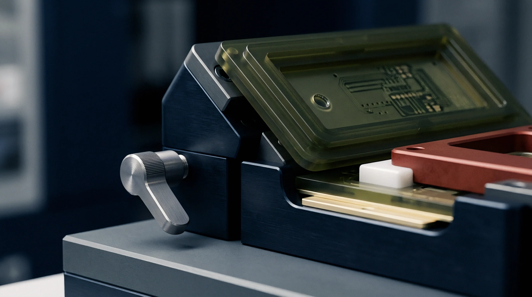
Calculated electric field enhancements at copper nodule peaks multiply nominal voltage stress up to twenty times, requiring profile-aware dielectric derating.

High-voltage copper characterization uses 3D spatial parameters to cap local peak roughness below two micrometers, preventing field enhancement breakdown.

Areal surface topography standardization for millimeter wave conductor loss prediction relies on ISO 25178 spatial bandwidth cutoffs and developed area ratio Sdr.
Substrate profile roughness shrinks effective copper conductivity at millimeter-wave frequencies, degrading waveguide quality factor and increasing cavity loss.

Ground layer conductive losses at high frequencies depend primarily on copper foil surface roughness profiles and reference current loop paths.
Expertise is a utility, not a secret. sentiention™ publishes its working knowledge as open reference: intelligence layer covering the materials it sources, the markets it enters, and the reference that serves both.