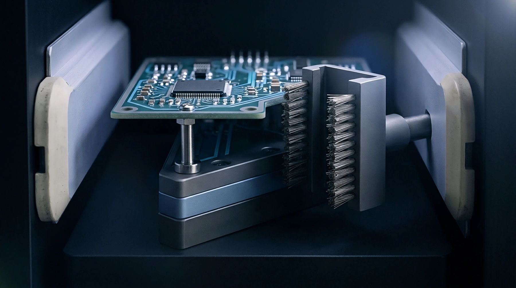
Integrating Boundary Scan Files with in Circuit Fixture Verification
Integrating boundary scan files into in-circuit fixtures reclaims blind BGA net coverage, cuts mechanical probe force, and lowers board diagnostic debug costs.
Integrating boundary scan files into in-circuit fixtures reclaims blind BGA net coverage, cuts mechanical probe force, and lowers board diagnostic debug costs.
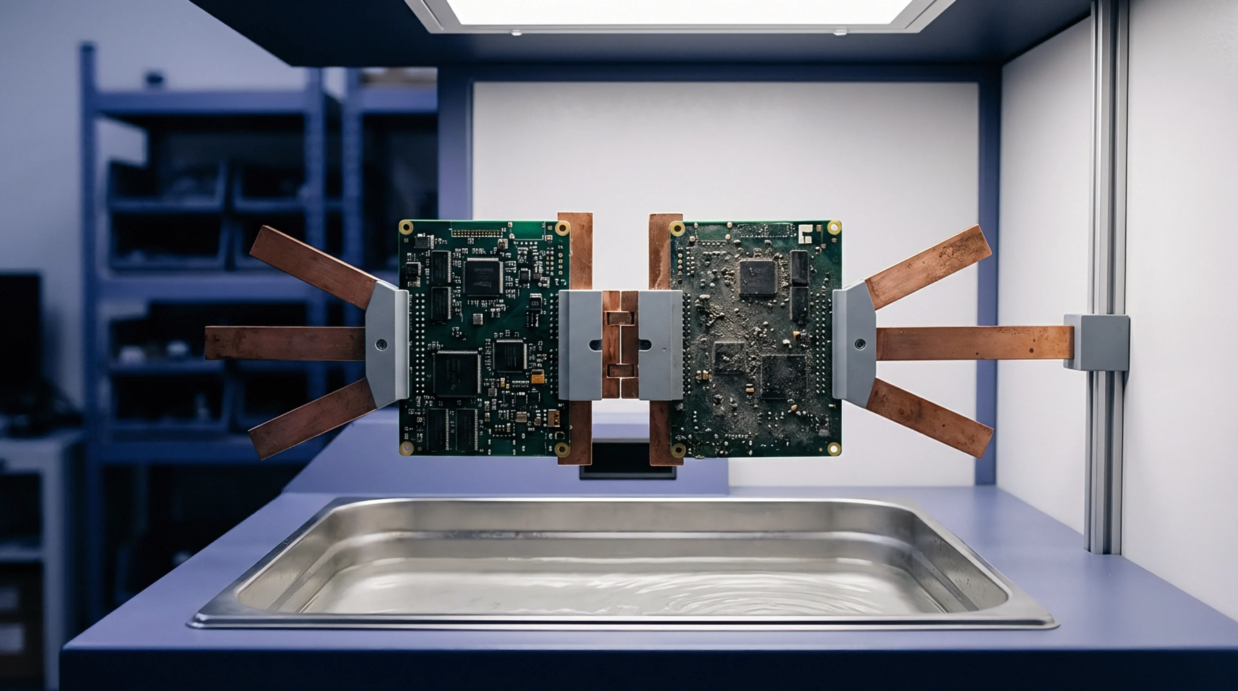
Configure clean TAP terminations, verify BSDL instruction registers, and execute EXTEST vectors to isolate physical solder bridges and open joints.

Three-dimensional regularized magnetic field inversion localizes subsurface microampere leakage channels across specific package layers, preventing scrap.

Fourier inverse Biot-Savart transformation deconvolves magnetic field arrays into planar PCB current maps to locate buried shorts without physical contact.

Planar magnetic field scanning isolates hidden multilayer current paths non-invasively, providing verifiable proof of assembly integrity.

Localized multi-pass rework drives extreme Z-axis dielectric expansion that shears microvia target pads, demanding in-situ Kelvin verification to catch latent opens.
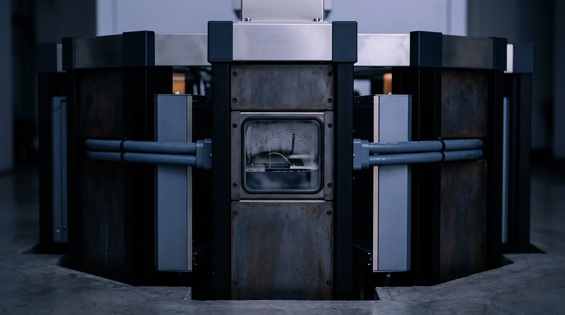
Multi-layer board rework demands strict preheating below glass transition, peak nozzle temperatures under 245 degrees Celsius, and a maximum of two thermal cycles.

Interconnect stress testing uses localized internal resistive heating to quantify via barrel fatigue and post separation caused by repeated rework cycles.

Calculating displacement currents and via fence boundary impedances limits high density interconnect cavity coupling and guarantees far field emissions compliance.
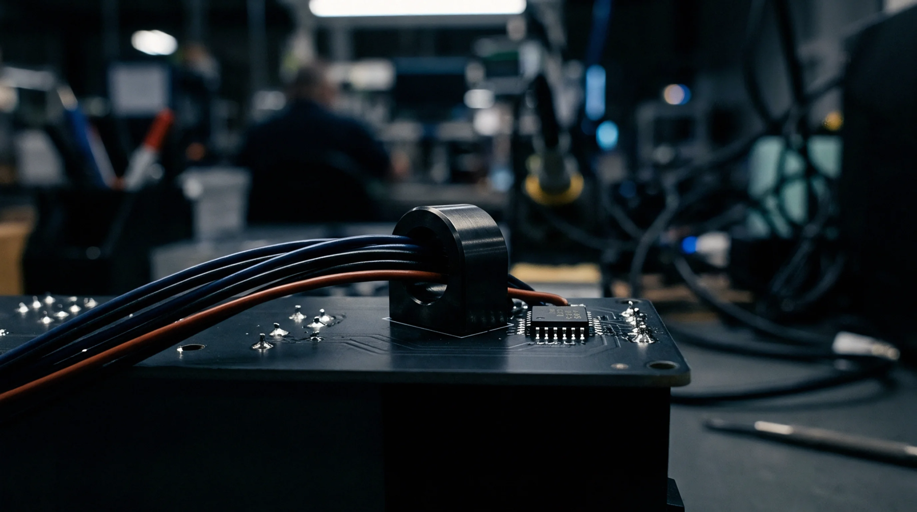
Phase-resolved near-field dipole reconstruction extracts complex source vectors to predict compliance radiated emissions without physical chamber bottlenecks.

Planar near-field scanning localizes high-frequency board currents and split-plane defects, isolating emission escapes before formal compliance chamber testing.
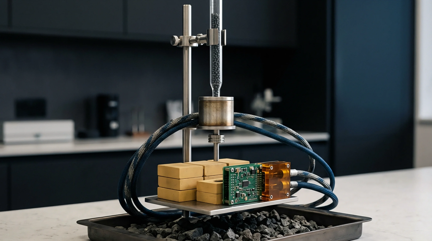
Interfacial solder joint voids accelerate creep strain accumulation, converting IPC-compliant connections into latent field open circuits.
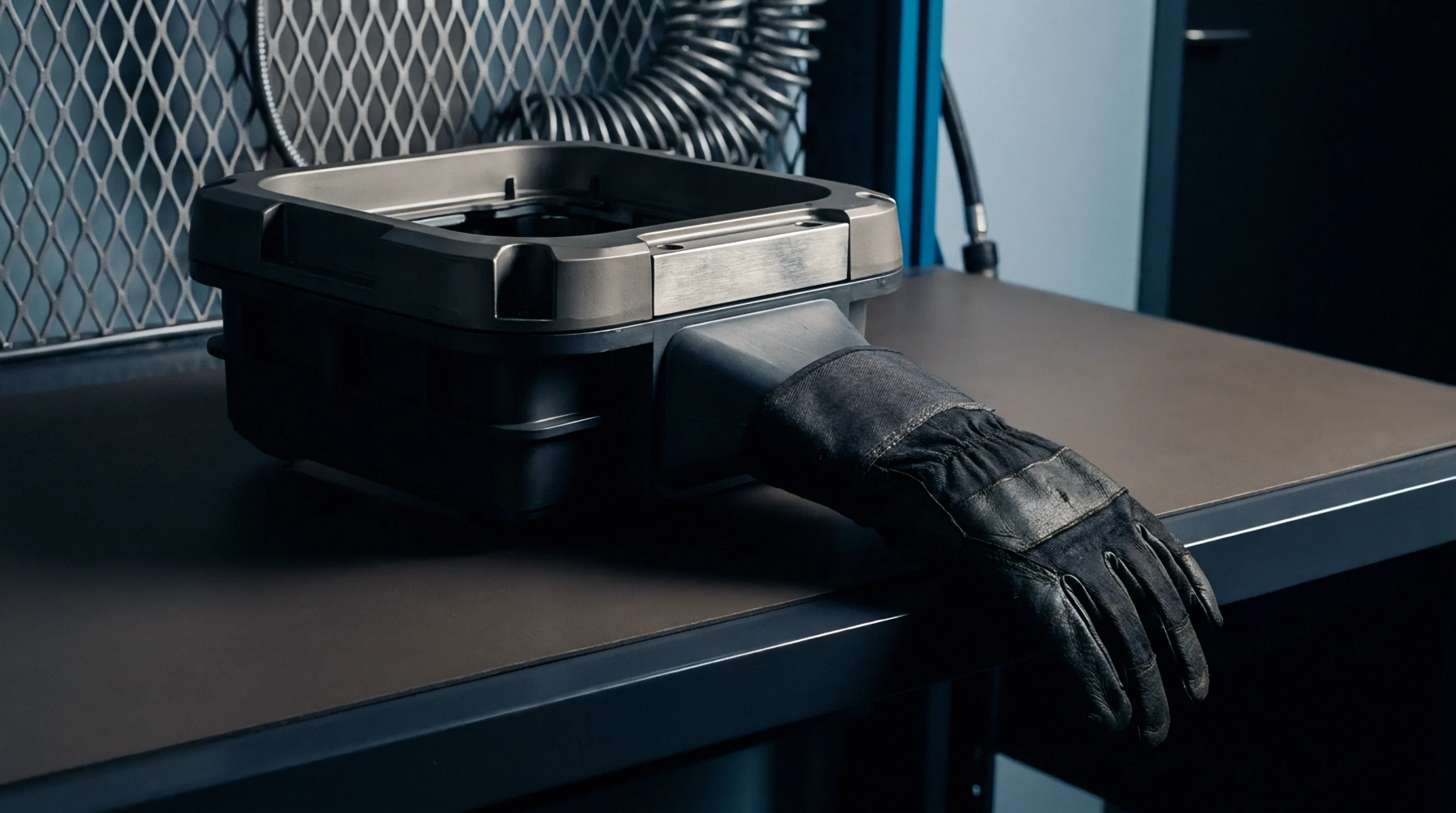
Boundary scan accessibility delivers over 95 percent structural interconnect coverage on high-density assemblies without physical bed-of-nails test probes.

High density defect classification demands isolating planar fractures and head-in-pillow anomalies through volumetric laminography and targeted thermal stress.

Microsection evaluation must confirm probe witness penetration stays confined to the gold and palladium cap without initiating microcracks in the nickel deposit.
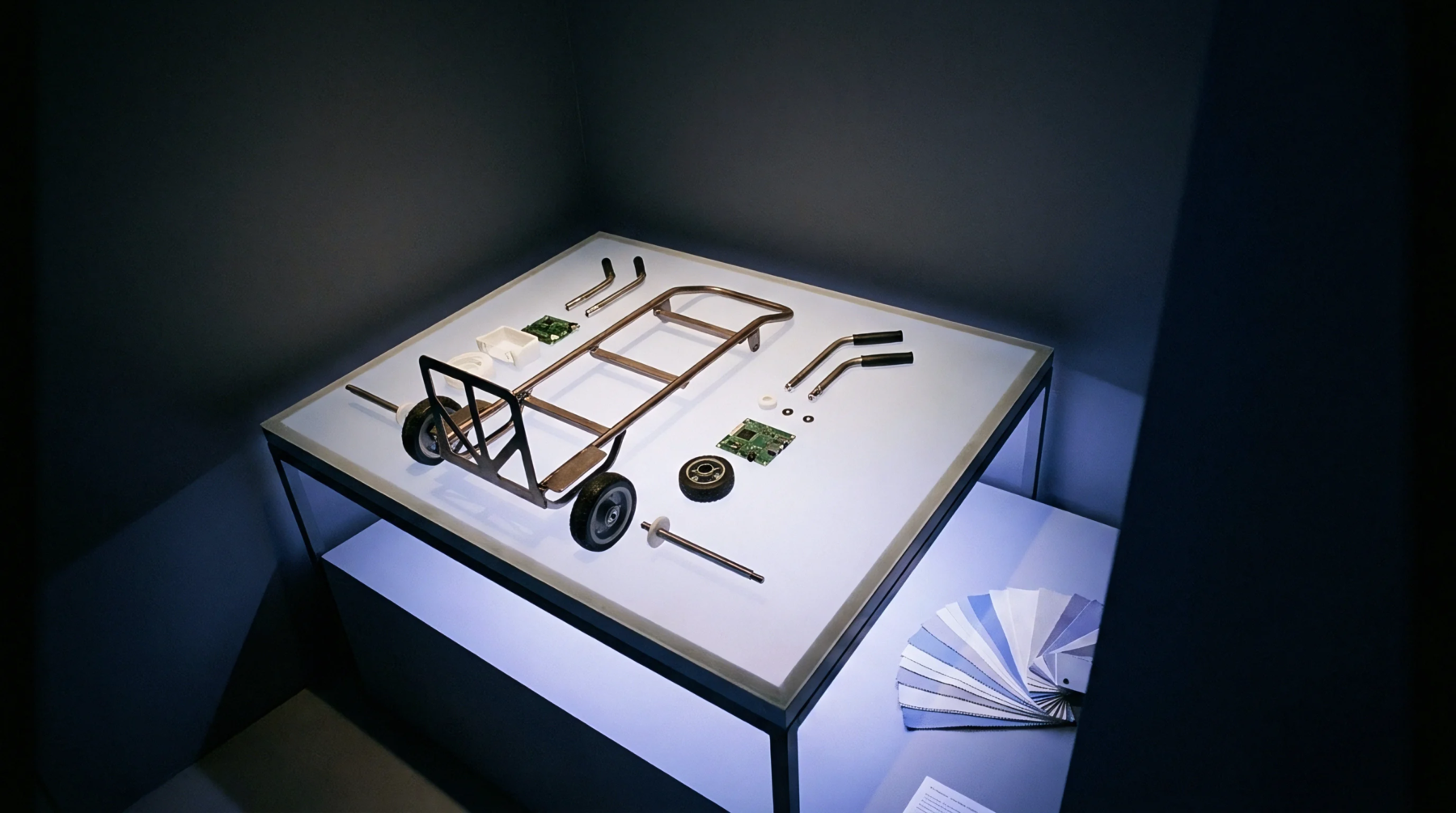
Controlled tip geometry and lateral scrub stabilize ENIG contact resistance while preventing false opens and deep dielectric damage on bare boards.

IPC-9252 test land placement demands exact probe diameters, stagger offsets, and mask clearances to secure full netlist coverage without board damage.
Statistically valid measurement uncertainty budgets defeat arbitrary border seizures by demonstrating that regulatory test results span legal compliance limits.
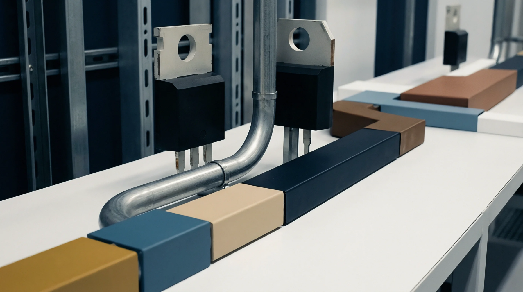
Align factory pre-shipment sampling with destructive customs laboratory thresholds to prevent border detentions, demurrage costs, and lot seizures.

Maintain complete technical construction files and sealed production golden samples to legally challenge and overturn border detentions within statutory deadlines.
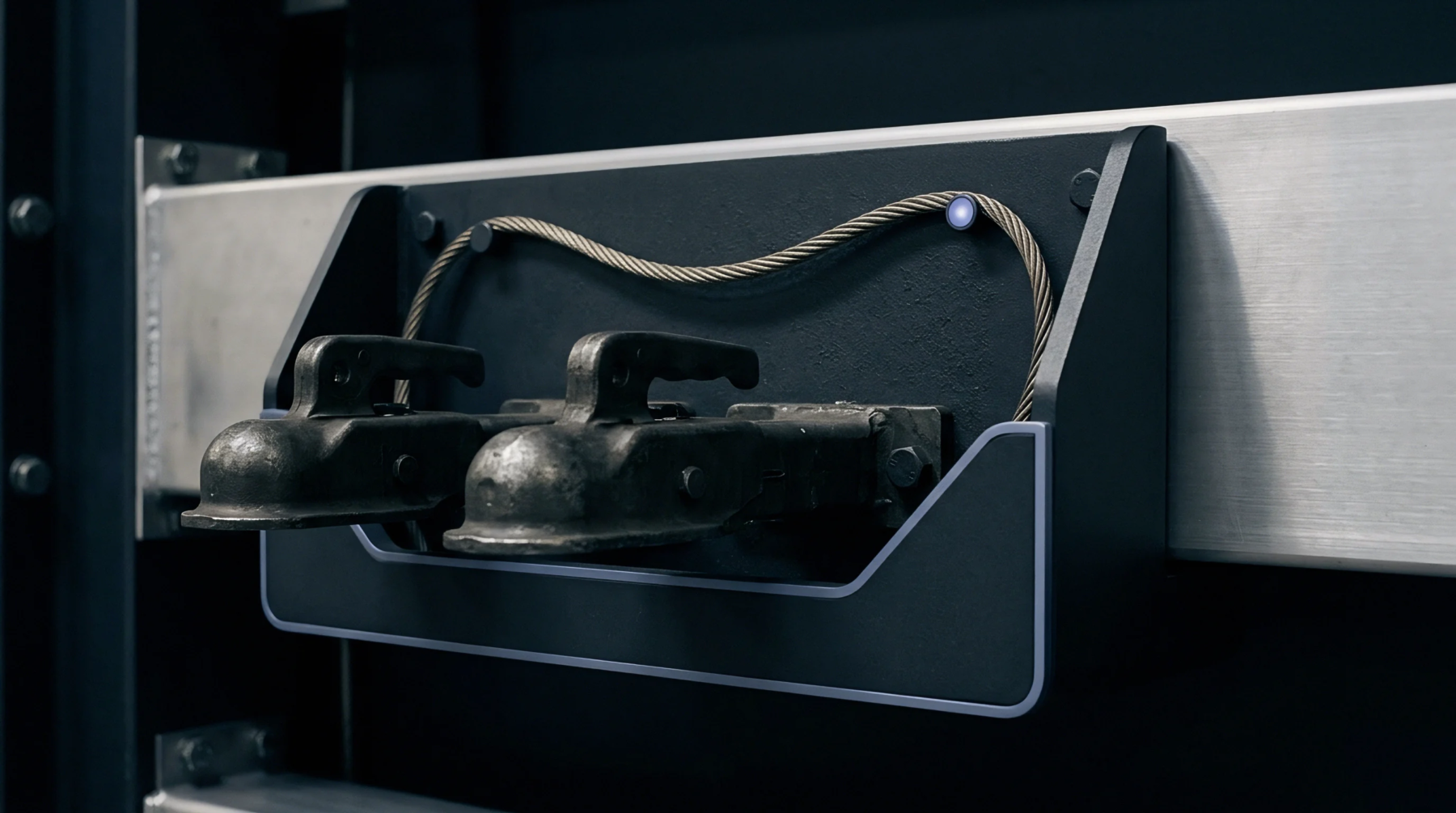
Dynamic in-situ monitoring during rapid thermal ramps separates unbuffered logic threshold dropouts from solder fatigue before boards escape to the field.
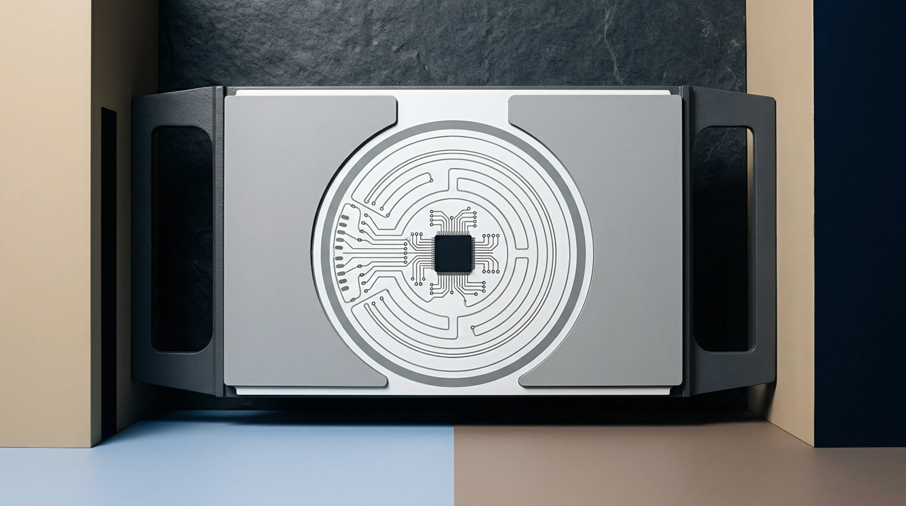
Boundary scan preconditioning isolates constrained nodes without test pads, allowing analog signature analysis to verify passive and junction integrity.
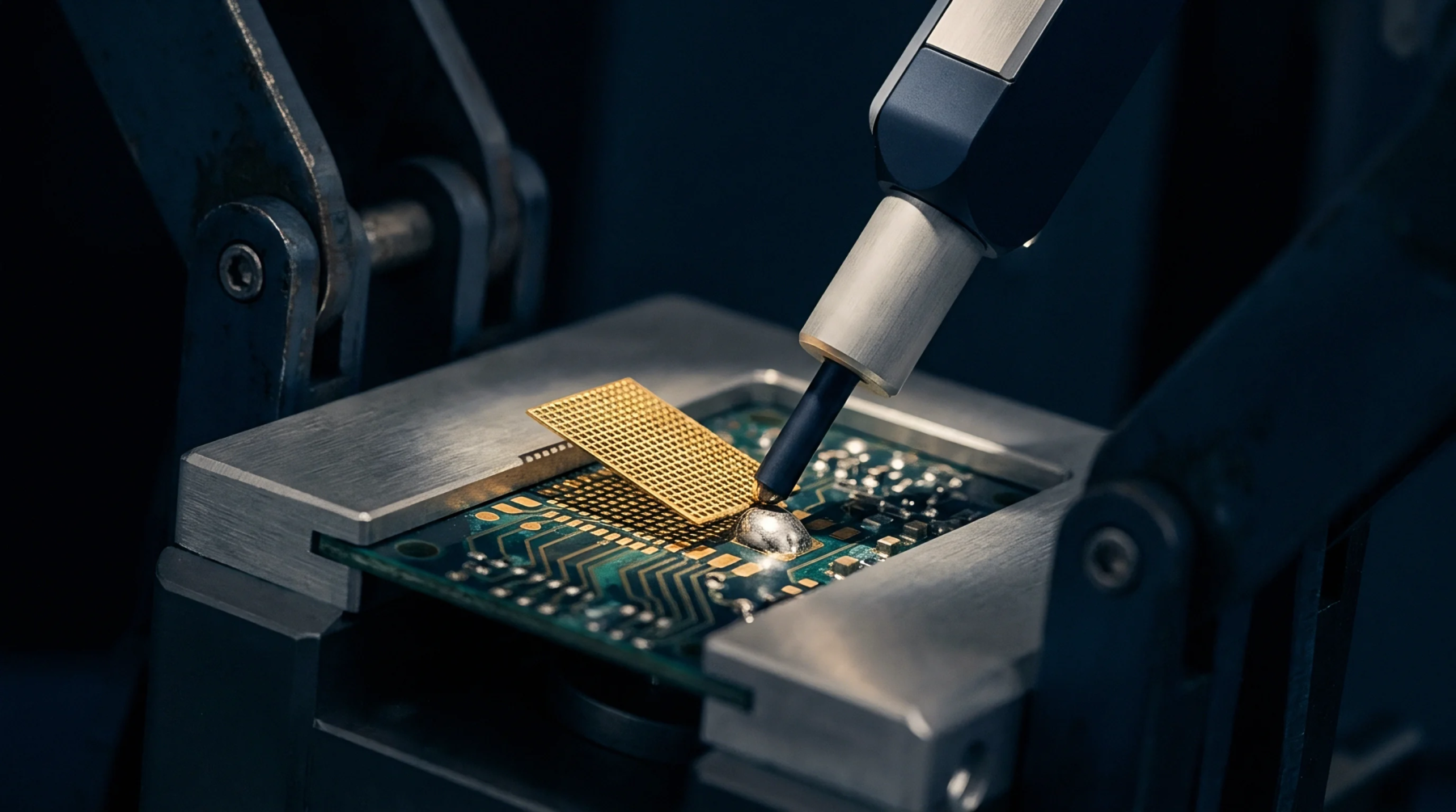
Verify structural fault coverage on high density assemblies by combining boundary scan with radiographic inspection where physical probe access falls below eighty percent.
Calibrating supersonic nozzle stagnation pressure sets the argon cluster size distribution, locking impact energy per atom to preserve interfacial chemistry.

Oblique neutral cluster processing directs momentum into tangential surface shear, preventing subsurface lattice damage and high-frequency trace attenuation.

Empirical silicon sputter yield quantification requires pairing optical crater volume metrology with mass-filtered Faraday cup cluster dosimetry.
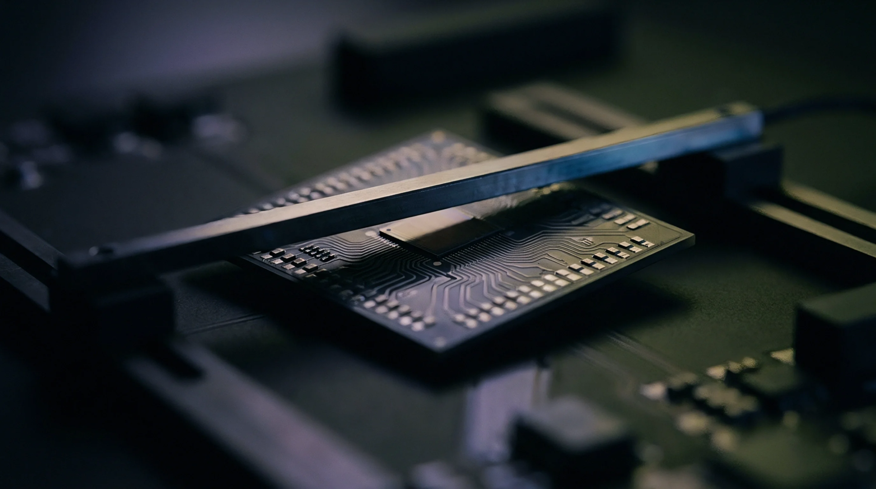
Latent copper-dielectric microcracks evade room-temperature factory testing, opening under operational heat to collapse high-speed receiver phase margins.
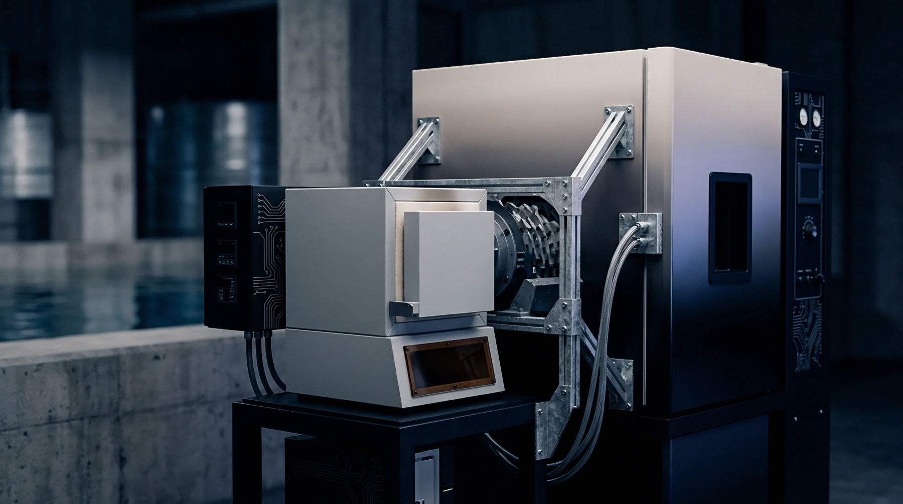
Differential channel skew drifts under environmental screening due to glass weave expansion mismatches, requiring in situ de-embedded phase verification.

Continuous high-speed resistance monitoring during thermal reflow simulation catches latent microvia void coalescence that passes room temperature checks.
Environmental temperature and humidity cycling degrades substrate integrated waveguide cavity damping by elevating loss tangents and fracturing via fences.
Expertise is a utility, not a secret. sentiention™ publishes its working knowledge as open reference: intelligence layer covering the materials it sources, the markets it enters, and the reference that serves both.