
Nickel Surface Finish Degradation of Microwave Cavity Quality Factors
Nickel finishes slash microwave cavity Q by contracting skin depth and introducing magnetic loss; maintain five skin depths of silver over non-magnetic barriers.
Nickel finishes slash microwave cavity Q by contracting skin depth and introducing magnetic loss; maintain five skin depths of silver over non-magnetic barriers.
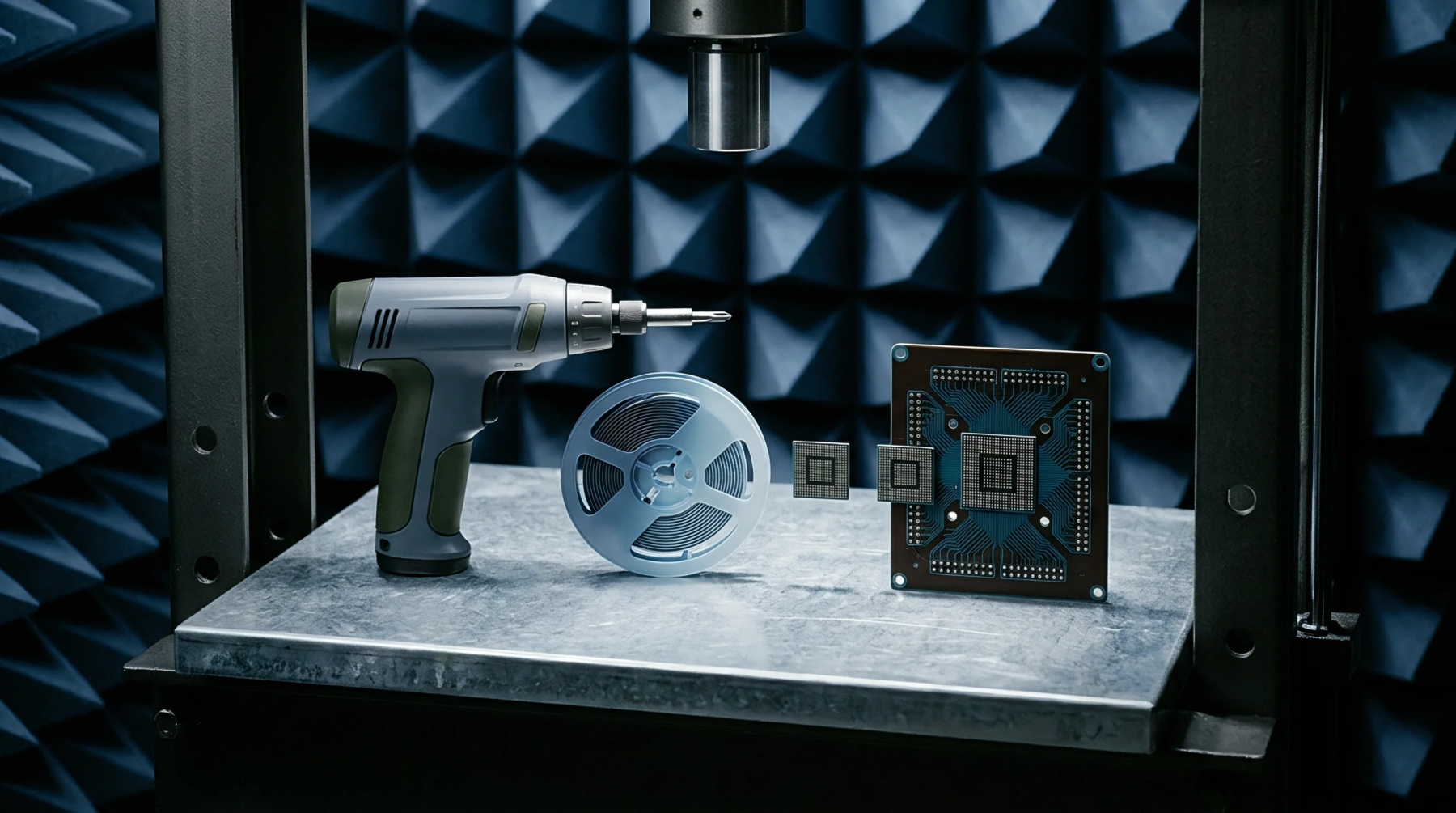
Select PCB cavity damping by tuning filler permeability to resonant field vectors, keeping dampers three trace heights away to prevent impedance drift.
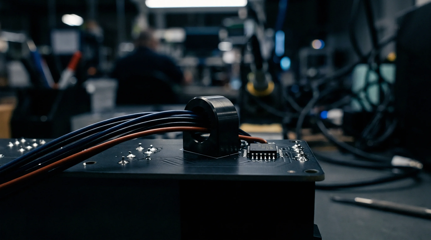
Substrate fatigue crack propagation rates depend on mode mixity and resin compliance, requiring continuous in situ resistance logging to prevent field escapes.
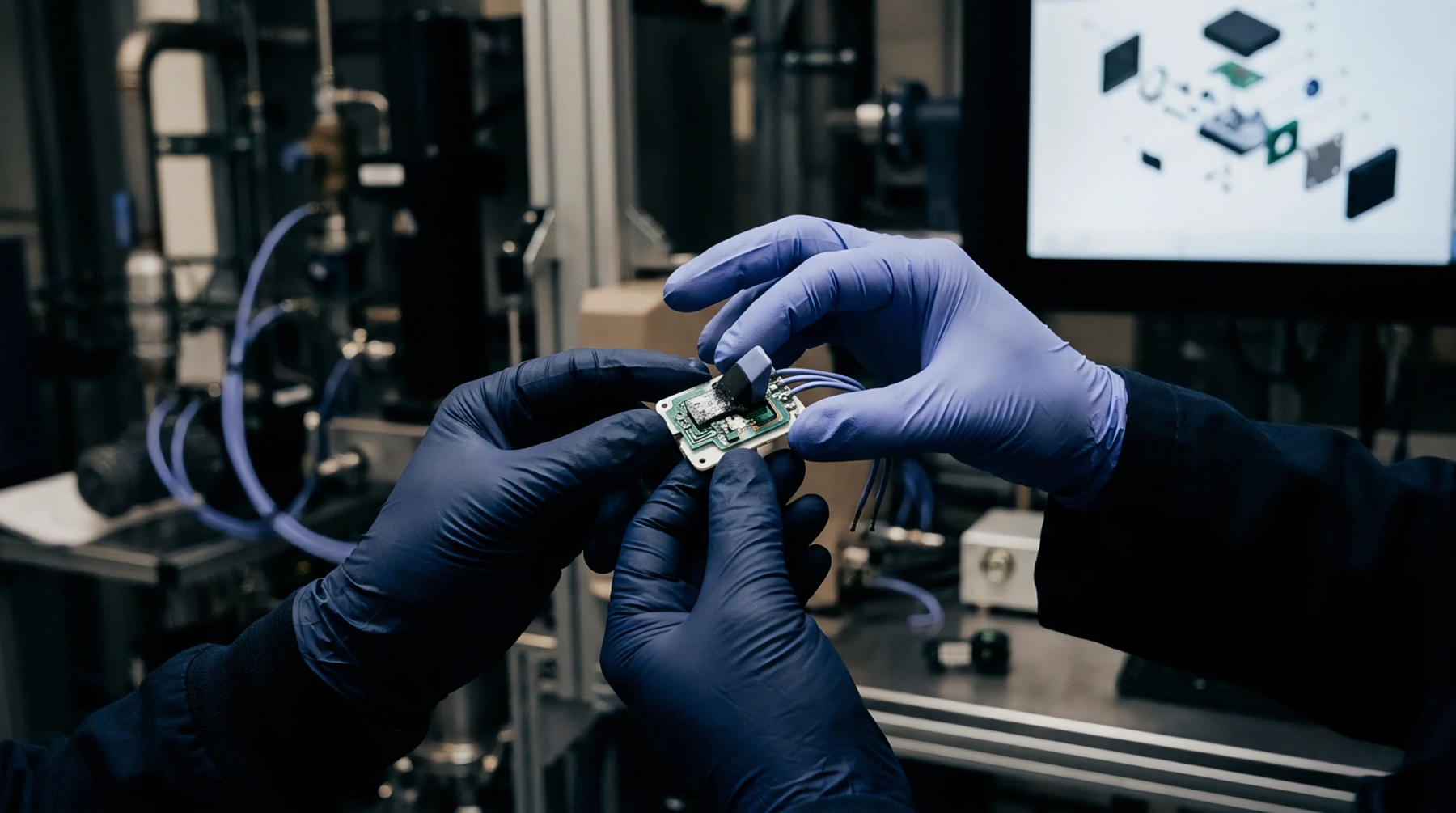
Dielectric micro-cracking lowers effective permittivity when dry but triples loss tangent under humidity, driving fatal RF attenuation shifts at high frequencies.
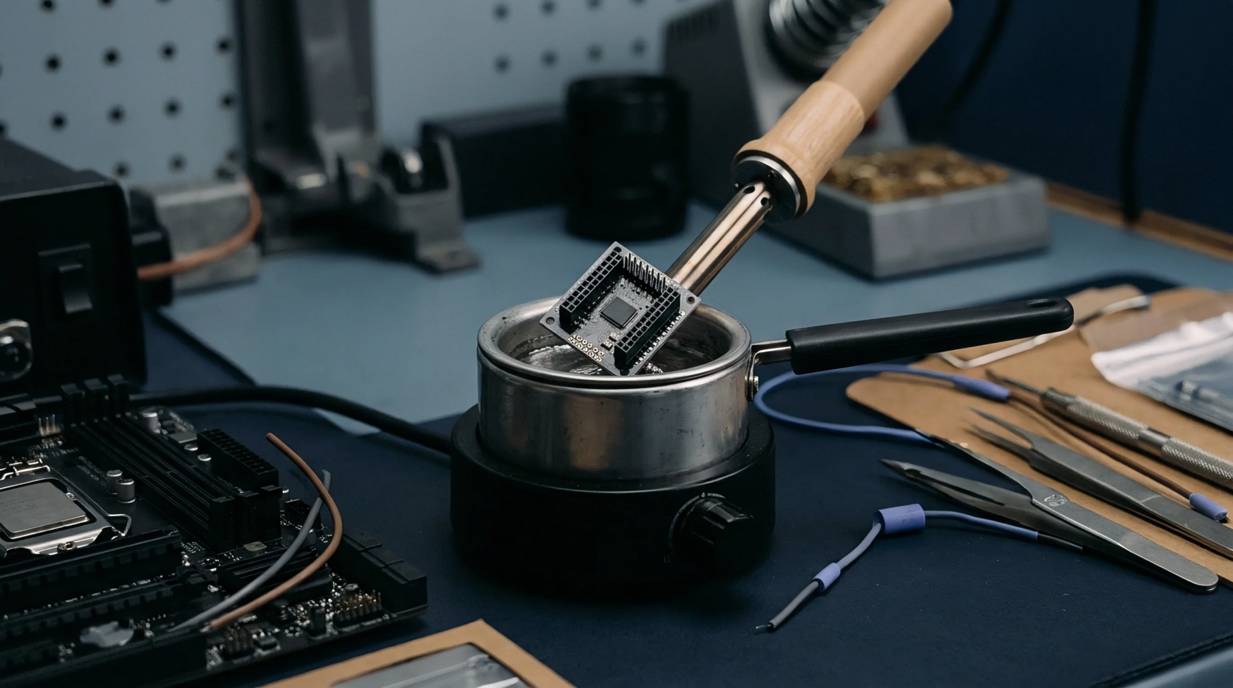
Peripheral via arrays fail via boundary shear driven by unconstrained resin expansion, demanding dummy guard vias and continuous dynamic thermal testing.

Edge emission escape through peripheral via gaps under transient switching loads depends on plane resonance and picket pitch.

Calculating perimeter via pitch below one-twentieth the guided harmonic wavelength maintains adequate shielding attenuation for radiated emissions compliance.

Suppression of plane cavity resonance relies on sub-lambda via fences, thin-core laminates, and edge damping to eliminate impedance peaks and radiated emissions.

Dynamic threshold shifts in hybrid vector probing resolve through settling delay insertion, pin heat tracking, and dynamic guardbanding.

Hardware triggers synchronizing probe tip mechanical settling with JTAG vectors eliminate false opens and bus contention on high-density circuit assemblies.

Optimizing boundary scan access for high-density interconnects replaces physical probes with silicon registers, maximizing fault coverage and lowering test cost.

Non-contact electron-beam and thermal radiometry verify sub-10-micrometer substrate nets, eliminating mechanical damage while securing packaging yield.
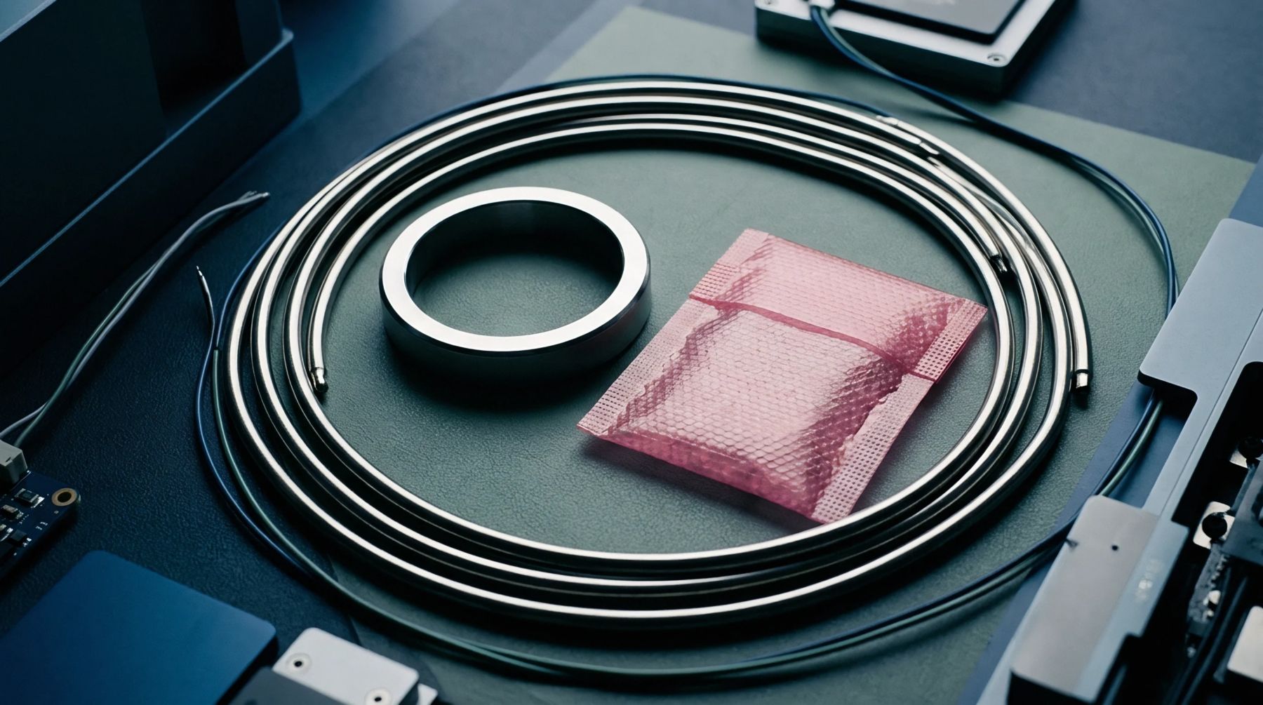
Flying probe capacitance screening locates open nets rapidly, while four-wire Kelvin micro-ohm verification isolates hidden trace necking and micro-via cracks.

High-density bare substrate continuity testing demands dynamic, geometry-derived resistance thresholds and four-wire Kelvin verification to prevent field failures.

Dynamic multi-domain scan capture causes transient voltage drops and false timing failures, requiring predictive parasitic modeling and vector-aware clock pacing.

Evaluating transient voltage drop during scan shift requires auditing vector toggle rates and on-die telemetry to eliminate false yield fallout.
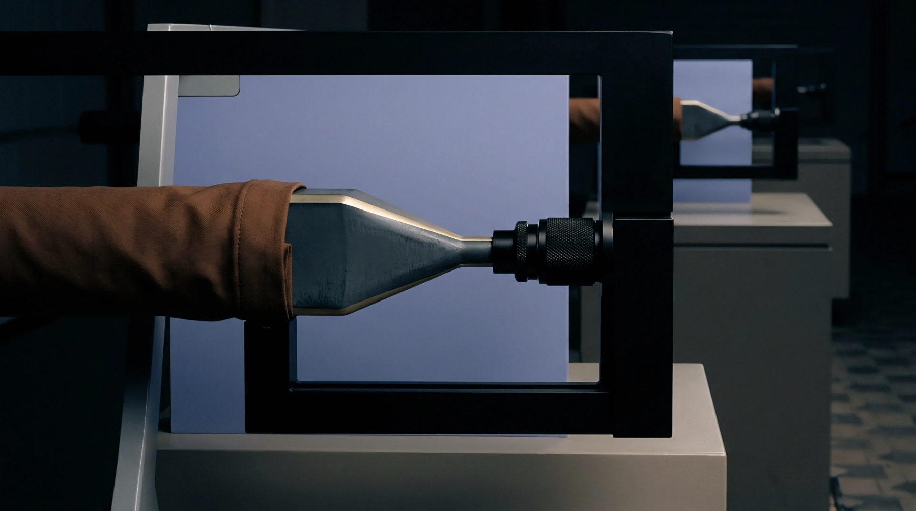
Extracting detailed coupled RC parasitic meshes for scan clock paths prevents unmodeled clock skew and shift hold violations from corrupting structural test logic.

Unshielded spring probes add parasitic loop inductance and contact noise that round TCK edges, causing boundary scan bit slips and costly false rejects.

Dynamic TAP contact resistance drift attenuates boundary scan signals, causing structural fault escapes that violate product conformity declarations.

Physical TAP probe contact mechanics dictate constriction resistance, where inadequate normal force and oxide films corrupt boundary scan signal integrity.

Combined boundary scan and bed-of-nails access modeling calculates structural escape rates to prevent latent defect exposure in field shipments.
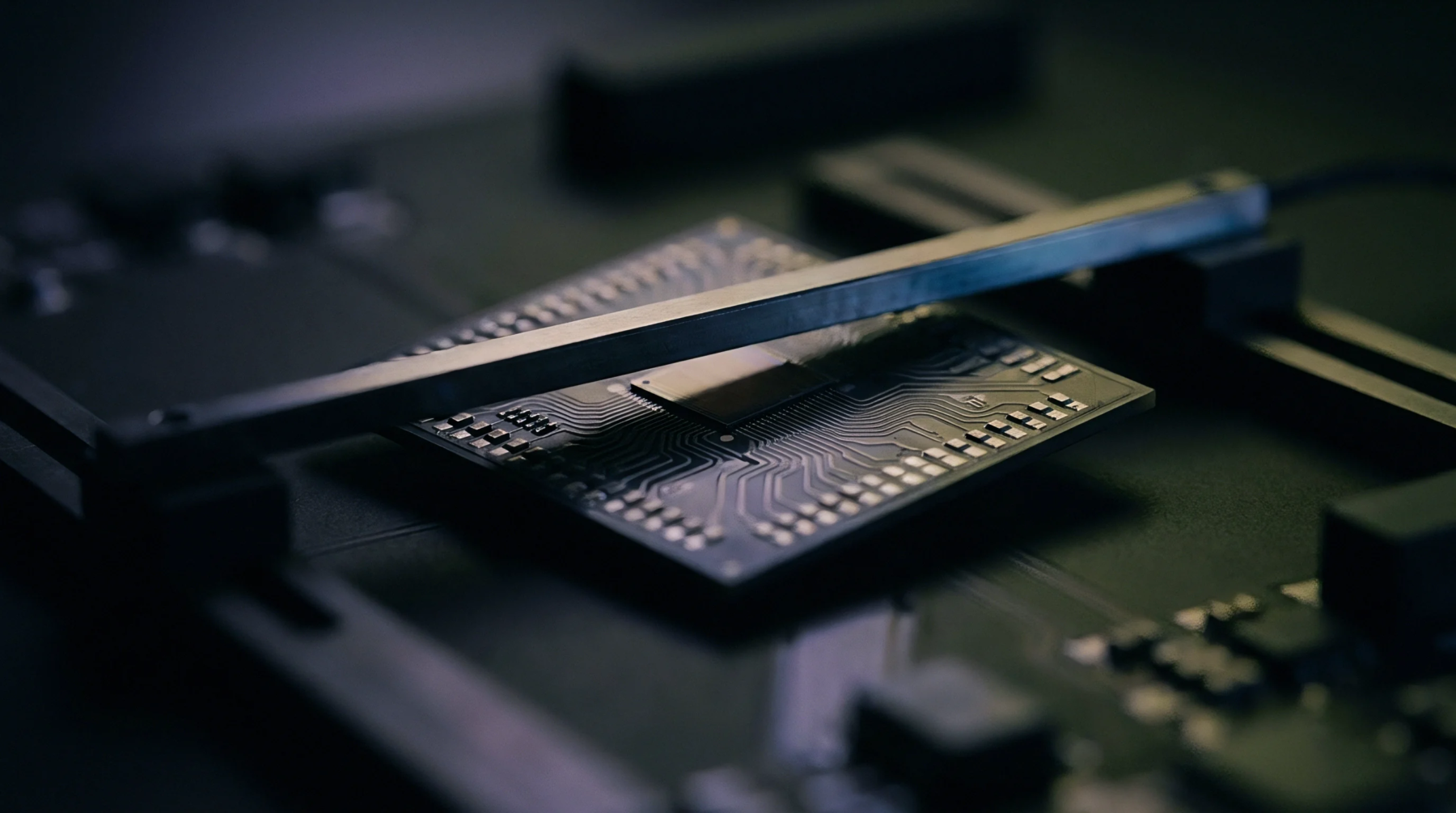
IEEE 1149.6 coverage derivation relies on RC decay bounds, receiver pulse timing, and precise AC open and short fault universe calculations.

Boundary scan replaces physical fixture probes by shifting serial test patterns through dedicated on-chip registers to prove high-density ASIC solder integrity.

Declare all engineering assists and match physical fixture capabilities to statutory export codes to prevent customs seizures and retroactive duty penalties.
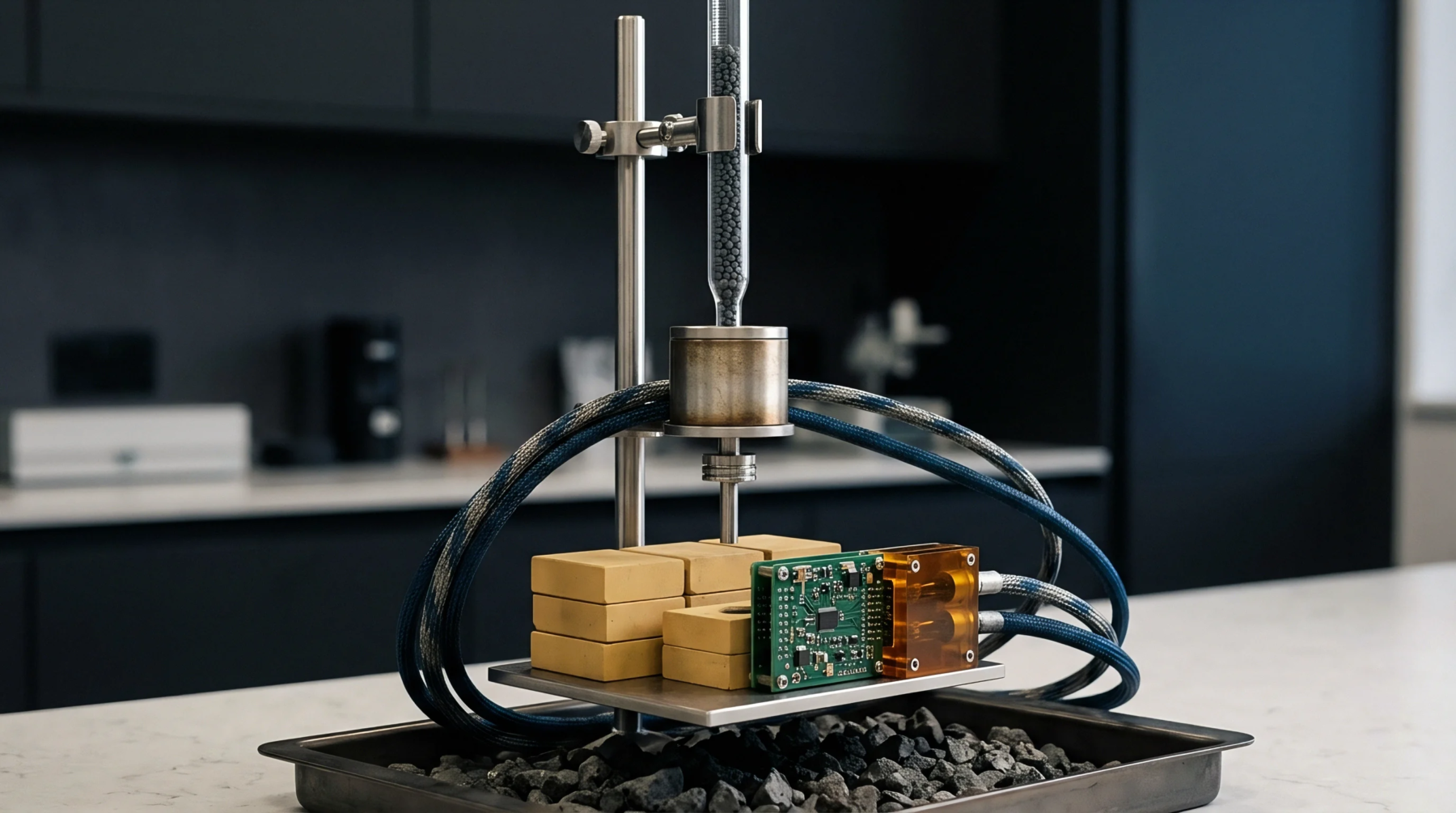
Transferring in-circuit test fixtures demands mechanical receiver alignment, guard loop settling verification, and fault-injection correlation to prevent escapes.
A technical asset handover protocol secures version-controlled test software, calibrated physical fixtures, and runoff data to transfer production without defect escapes.
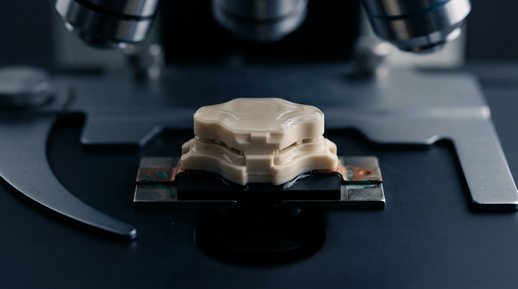
Diagnosing intermittent microvia defects requires continuous high-bandwidth resistance monitoring during simultaneous mechanical flexure and thermal cycling.

Non-redundant aggregation of optical, X-ray, and boundary scan coverage metrics determines true defect escape risk on high-density circuit boards.

Boundary scan pin coverage metrics require verified BSDL models, segmented chains, and strict fault denominators to prevent latent solder defects escaping.

IEEE 1149.6 boundary scan isolates AC-coupled opens and shorts but misses partial solder voids and high-frequency channel losses that demand at-speed testing.
Expertise is a utility, not a secret. sentiention™ publishes its working knowledge as open reference: intelligence layer covering the materials it sources, the markets it enters, and the reference that serves both.