Signal Magnitude
Ratio measurements quantify energy transmission and reflection across high frequency interconnects within radio frequency or microwave circuitry. These s-parameters map the linear network behavior by comparing the complex voltage waves traveling toward and away from a multi-port device. Fabrication houses verify these values through vector network analyzers during post-production validation to ensure impedance matching across transmission lines.
Deviations from target return loss suggest dielectric inconsistencies or variations in trace geometry that degrade signal integrity in high speed digital hardware.
Interconnect Performance
Validation protocols require these measurements to isolate physical layer failures from logic errors during prototyping cycles. A design team defines acceptable margins for insertion loss based on the allowable power budget of the intended application. Engineers confirm that measured return loss values stay below specified thresholds to avoid signal reflections that introduce crosstalk or jitter into the communication channel.
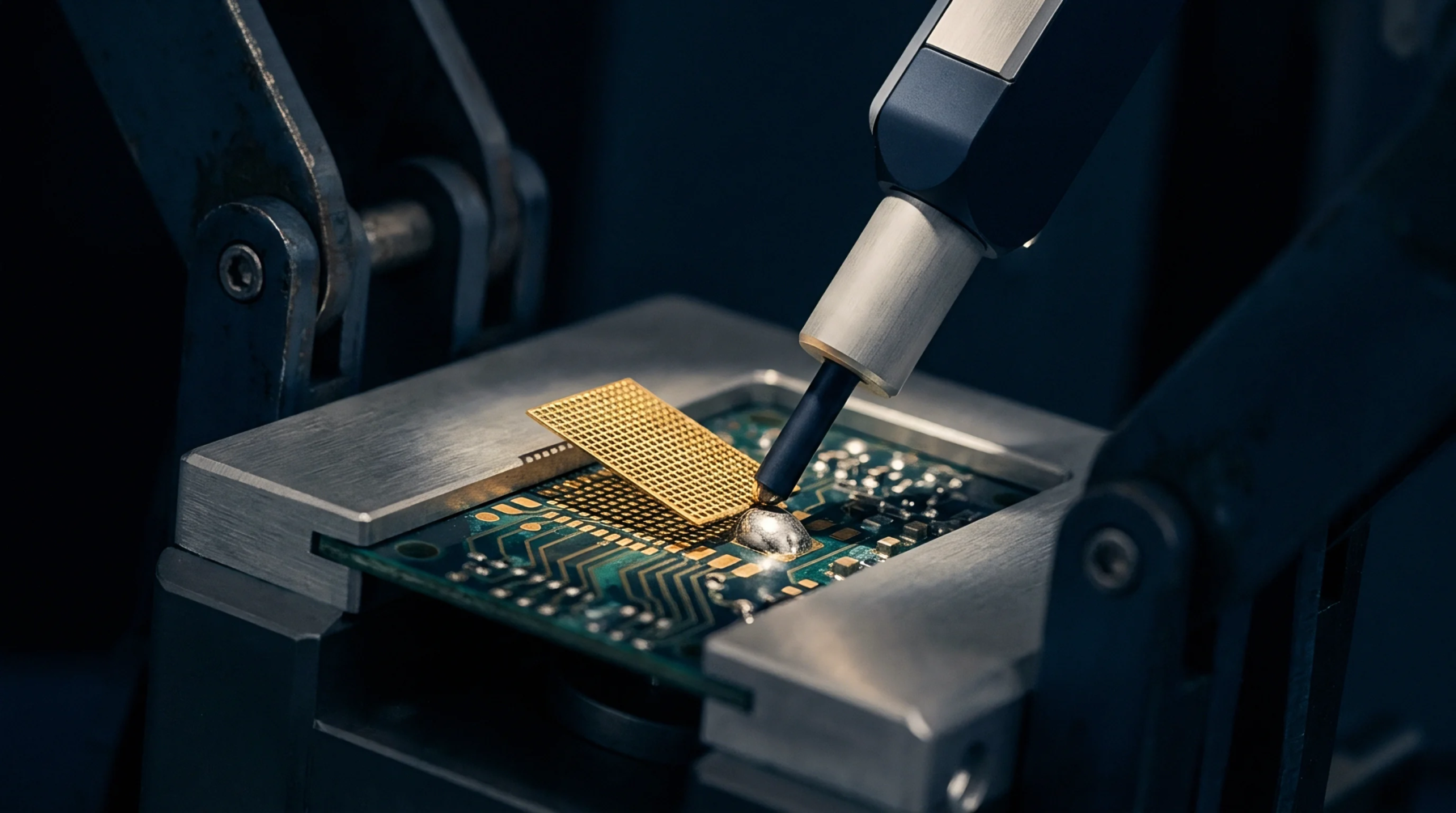
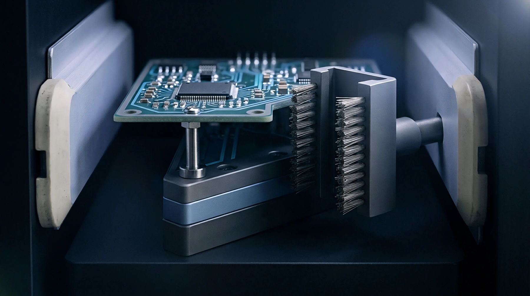
If a trace width narrows due to over-etching, the impedance mismatch changes the reflected power ratio, which the analyzer detects as a shift in magnitude at a specific frequency point. Surface mount component pads also alter the local impedance, requiring compensation to maintain continuity throughout the signal path. Automated test fixtures hold the board at fixed contact points to minimize parasitic capacitance that could skew data acquisition.
Consistent data sets allow manufacturers to verify if material thickness meets the nominal requirements for controlled impedance environments. Tight process control over lamination cycles reduces the variance between boards, ensuring that every assembly functions according to the original layout specifications.
Verification Requirement
Inspection standards mandate s-parameter documentation for critical boards where signal frequencies exceed five gigahertz. This requirement prevents mounting populated modules on substrates that contain hidden manufacturing defects. Production teams reject boards when the measured scattering matrix deviates from simulated models beyond the stated tolerances.
Precise characterization confirms that each layer stackup effectively guides electromagnetic waves without undue attenuation. Measurement accuracy depends upon proper calibration of the test hardware to account for cable losses and probe artifacts. Validated s-parameters confirm the electrical reliability of the completed assembly.