Pattern Fidelity
Photolithographic exposure technology utilizing a digitally modulated ultraviolet laser scans circuit layouts directly onto a photosensitive photoresist coated copper substrate without relying on physical photomasks. Laser direct imaging eliminates tooling costs and registration errors inherent in traditional glass mask production, granting fabricators immediate design revision capability during inner layer processing. Registration accuracy improves because optical scaling algorithms compensate for material expansion and shrinkage during high temperature pressing cycles before etching.
Production tooling departments translate computer aided design Gerber files into raster data formats, driving high speed polygon mirror scanners across laminated panel surfaces. Photosensitive dry film resists polymerize locally under focused photon energy, defining high density traces and fine pitch pad geometries for advanced multichayer printed circuit boards. Optical power density and exposure wavelength must match photoresist sensitivity curves precisely, preventing undercutting or incomplete polymerization through thick copper foil structures.
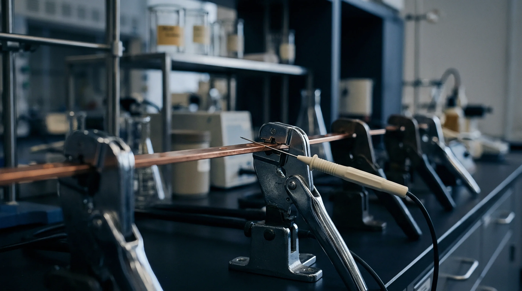
Substrate handling systems clamp panels via pneumatic registration pins, minimizing mechanical vibration artifacts during high speed raster sweeps. Automated optical inspection equipment subsequently verifies patterned conductor widths against original CAD intent, catching opens, shorts, and line width anomalies before chemical etching removes unwanted copper.
Thermal Stability
Dimensional variation across woven fiberglass reinforced epoxy laminates during multi-step fabrication introduces registration failure modes that direct laser exposure mitigates through real time spatial scaling. Panel temperature fluctuations inside the exposure chamber induce localized expansion, requiring optical systems to measure fiducial markers and dynamically distorting raster scans to match actual copper coordinates. Etching yields depend entirely on this precise geometric alignment between sequential conductive layers, particularly when outer layer features must land atop buried microvias with twenty micron positional tolerances.
Mechanical press cycles compress resin matrices unevenly, yielding anisotropic substrate deformation that static phototools cannot accommodate without generating systematic bridging or breakout defects. Software compensations calculate distinct stretch vectors for orthogonal axes, adjusting galvanometer mirror deflections on a panel by panel basis during exposure.
Process Economics
Capital expenditure amortisation models shift away from consumable chrome on glass photomasks toward high throughput digital switching hardware when fabrication facilities adopt maskless exposure workflows for high mix production lines. Setup times drop significantly because engineering change orders upload straight to the exposure controller without waiting for external mask fabrication or physical tooling verification runs. Yield enhancement arises from removing physical contact between emulsion surfaces and dry film resists, eliminating particle entrapment defects that cause localized etching shorts on fine pitch surface mount technology footprints.
Maintenance overhead concentrates on optical component cleanliness and laser diode calibration stability rather than dry room humidity control for fragile emulsion master plates. Operational margins stabilize across small batch runs because prototype iterations incur zero tooling penalties, matching the economic demands of modern electronic contract manufacturing environments.